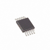
DS3502U+T&R Maxim Integrated Products, DS3502U+T&R Datasheet - Page 7

DS3502U+T&R
Manufacturer Part Number
DS3502U+T&R
Description
IC POT DGTL NV 128TAP 10-MSOP
Manufacturer
Maxim Integrated Products
Datasheet
1.DS3502UTR.pdf
(11 pages)
Specifications of DS3502U+T&R
Taps
128
Resistance (ohms)
10K
Number Of Circuits
1
Temperature Coefficient
±4ppm/°C
Memory Type
Non-Volatile
Interface
I²C, 2-Wire Serial
Voltage - Supply
2.5 V ~ 5.5 V
Operating Temperature
-40°C ~ 100°C
Mounting Type
Surface Mount
Package / Case
10-MSOP, Micro10™, 10-uMAX, 10-uSOP
Resistance In Ohms
10K
Lead Free Status / RoHS Status
Lead free / RoHS Compliant
The slave address byte consists of a 7-bit slave
address plus a R/W bit (see Figure 1). The DS3502’s
slave address is determined by the state of the A0 and
A1 address pins. These pins allow up to four devices to
reside on the same I
result in a 0 in the corresponding bit position in the
slave address. Conversely, address pins tied to V
result in a 1 in the corresponding bit positions. For
example, the DS3502’s slave address byte is 50h when
A0 and A1 pins are grounded. I
described in detail in the I
Description section.
The following terminology is commonly used to describe
I
Characteristics table for additional information.)
Master device: The master device controls the slave
devices on the bus. The master device generates SCL
clock pulses and START and STOP conditions.
Figure 1. DS3502 Slave Address Byte
Figure 2. I 2 C Timing Diagram
2
C data transfers. (See Figure 2 and the I
SDA
SCL
NOTE: TIMING IS REFERENCED TO V
I
2
Slave Address Byte and Address Pins
*THE SLAVE ADDRESS IS DETERMINED BY ADDRESS PINS A0, A1.
STOP
C Serial Interface Description
MSB
t
BUF
0
START
1
_______________________________________________________________________________________
2
C bus. Address pins tied to GND
SLAVE ADDRESS*
0
IL(MAX)
t
t
HD:STA
LOW
1
AND V
0
IH(MIN)
2
2
C Serial Interface
C communication is
A1
.
I
t
2
R
t
HD:DAT
C Definitions
2
A0
C AC Electrical
LSB
R/W
t
F
t
HIGH
CC
High-Voltage, NV, I
t
SU:DAT
Slave devices: Slave devices send and receive data at
the master’s request.
Bus idle or not busy: Time between STOP and START
conditions when both SDA and SCL are inactive and in
their logic-high states.
START condition: A START condition is generated by
the master to initiate a new data transfer with a slave.
Transitioning SDA from high to low while SCL remains
high generates a START condition.
STOP condition: A STOP condition is generated by
the master to end a data transfer with a slave.
Transitioning SDA from low to high while SCL remains
high generates a STOP condition.
Repeated START condition: The master can use a
repeated START condition at the end of one data trans-
fer to indicate that it will immediately initiate a new data
transfer following the current one. Repeated STARTS are
commonly used during read operations to identify a spe-
cific memory address to begin a data transfer. A repeat-
ed START condition is issued identically to a normal
START condition.
Bit write: Transitions of SDA must occur during the low
state of SCL. The data on SDA must remain valid and
unchanged during the entire high pulse of SCL plus the
setup and hold time requirements. Data is shifted into the
device during the rising edge of the SCL.
Bit read: At the end of a write operation, the master
must release the SDA bus line for the proper amount of
setup time before the next rising edge of SCL during a
bit read. The device shifts out each bit of data on SDA
at the falling edge of the previous SCL pulse and the
REPEATED
START
t
SU:STA
t
HD:STA
t
SP
2
C POT
t
SU:STO
7


