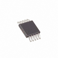
DS3906U+T&R Maxim Integrated Products, DS3906U+T&R Datasheet - Page 12

DS3906U+T&R
Manufacturer Part Number
DS3906U+T&R
Description
IC RESIST VAR TRPL 10USOP
Manufacturer
Maxim Integrated Products
Datasheet
1.DS3906U.pdf
(14 pages)
Specifications of DS3906U+T&R
Taps
64
Resistance (ohms)
1.45K, 2.54K, 2.54K
Number Of Circuits
3
Temperature Coefficient
60 ppm/°C Typical
Memory Type
Non-Volatile
Interface
I²C, 2-Wire Serial
Voltage - Supply
2.7 V ~ 5.5 V
Operating Temperature
-40°C ~ 85°C
Mounting Type
Surface Mount
Package / Case
10-MSOP, Micro10™, 10-uMAX, 10-uSOP
Resistance In Ohms
1.45K, 2.54K, 2.54K
Lead Free Status / RoHS Status
Lead free / RoHS Compliant
Acknowledge Polling: Any time an EEPROM page is
written, the DS3906 requires the EEPROM write time
(t
page to EEPROM. During the EEPROM write time, the
device does not acknowledge its slave address
because it is busy. It is possible to take advantage of
this phenomenon by repeatedly addressing the
DS3906, which allows communication to continue as
soon as the DS3906 is ready. The alternative to
acknowledge polling is to wait for a maximum period of
t
EEPROM Write Cycles: When EEPROM writes occur,
the DS3906 internally writes the whole EEPROM page (2-
bytes) even if only a single byte write was performed.
Writes that do not modify all 2 bytes on the page are
valid and do not corrupt any of other bytes on the same
page. Because the whole page is written, even bytes on
the page that were not modified during the transaction
are still subject to a write cycle. The DS3906’s EEPROM
write cycles are specified in the Nonvolatile Memory
Characteristics table. The specification shown is at the
worst-case temperature. It is capable of handling many
additional writes at room temperature.
Triple NV Low Step Size Variable
Resistor Plus Memory
Figure 3. I
12
W
W
to elapse before attempting to access the device.
) after the stop condition to write the contents of the
TYPICAL I
START
____________________________________________________________________
E)
A)
B)
C)
D)
EXAMPLE I
TWO BYTE READ
-READ TWO BYTES OF
USER EEPROM
STARTING
SINGLE BYTE WRITE
-WRITE RESISTOR 1
TO 00h
SINGLE BYTE READ
-READ RESISTOR 0
SINGLE BYTE WRITE
-WRITE FIRST BYTE OF
USER EEPROM TO FFh
TWO BYTE WRITE
-WRITE TWO BYTES OF
FROM 00h
USER EEPROM TO 00h
2
C Communication Examples
MSB
2
1
C WRITE TRANSACTION
2
C TRANSACTIONS (WHEN A0, A1, AND A2 ARE CONNECTED TO GND)
0
1
ADDRESS*
SLAVE
START
START
START 1 0 1 0 0 0 0 0
START
START
0
A2
1 0 1 0 0 0 0 0
1 0 1 0 0 0 0 0
1 0 1 0 0 0 0 0
1 0 1 0 0 0 0 0
A1
A0h
A0h
A0h
A0h
A0h
A0
WRITE
READ/
R/W
LSB
SLAVE
SLAVE
SLAVE
SLAVE
SLAVE
ACK
ACK
ACK
ACK
ACK
SLAVE
ACK
1 1 1 1 1 0 0 1
0 0 0 0 0 0 0 0
1 1 1 1 1 0 0 0
0 0 0 0 0 0 0 0
0 0 0 0 0 0 0 0
MSB
F9h
F8h
00h
00h
00h
b7
b6
REGISTER/MEMORY ADDRESS
SLAVE
SLAVE
SLAVE
SLAVE
*THE SLAVE ADDRESS IS DETERMINED BY ADDRESS PINS A0, A1, AND A2.
SLAVE
b5
ACK
ACK
ACK
ACK
ACK
b4
1 1 1 1 1 1 1 1
0 0 0 0 0 0 0 0
0 0 0 0 0 0 0 0
REPEATED
REPEATED
START
START
b3
FFh
00h
b2
Reading a Single Byte from a Slave: Unlike the write
operation that uses the specified memory address byte
to define where the data is to be written, the read oper-
ation occurs at the present value of the memory
address counter. To read a single byte from the slave,
the master generates a start condition, writes the slave
address byte with R/W = 1, reads the data byte with a
NACK to indicate the end of the transfer, and generates
a stop condition. However, since requiring the master
to keep track of the memory address counter is imprac-
tical, the following method should be used to perform
reads from a specified memory location.
Manipulating the Address Counter for Reads: A
dummy write cycle can be used to force the address
counter to a particular value. To do this the master gen-
erates a start condition, writes the slave address byte
(R/W =0), writes the memory address where it desires
to read, generates a repeated start condition, writes the
slave address byte (R/W = 1), reads data with ACK or
NACK as applicable, and generates a stop condition.
See Figure 3 for a read example using the repeated
start condition to specify the starting memory location.
1 0 1 0 0 0 0 1
1 0 1 0 0 0 0 1
b1
SLAVE
SLAVE
SLAVE
ACK
ACK
ACK
A1h
A1h
LSB
b0
0 0 0 0 0 0 0 0
STOP
SLAVE
STOP
ACK
00h
SLAVE
SLAVE
ACK
ACK
MSB
b7
LOCATION 00h
SLAVE
b6
ACK
DATA
DATA
RES 0
b5
STOP
b4
MASTER
DATA
MASTER
NACK
ACK
b3
LOCATION 01h
b2
STOP
DATA
b1
LSB
b0
MASTER
SLAVE
NACK
ACK
STOP
STOP


