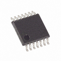
DS1845E-050+T&R Maxim Integrated Products, DS1845E-050+T&R Datasheet

DS1845E-050+T&R
Specifications of DS1845E-050+T&R
Related parts for DS1845E-050+T&R
DS1845E-050+T&R Summary of contents
Page 1
FEATURES § Two linear taper potentiometers - DS1845-010 one 10k, 100 position & one 10k, 256 position - DS1845-050 one 10k, 100 position & one 50k, 256 postition - DS1845-100 one 10k, 100 position & one 100k, 256 position ...
Page 2
PIN DESCRIPTIONS Name TSSOP BGA GND 7 D1 SDA 1 B2 SCL ...
Page 3
DS1845 BLOCK DIAGRAM Figure 1 VCC 2-WIRE INTERFACE GND SDA SCL MEMORY ORGANIZATION The DS1845’s serial EEPROM is internally organized with 256 words of 1 byte each. Each word requires an 8-bit address for random word ...
Page 4
Interface Reset: After any interruption in protocol, power loss, or system reset, the following steps reset the DS1845. 1. Clock up to nine cycles. 2. Look for SDA high in each cycle while SCL is high. 3. Create a ...
Page 5
CURRENT ADDRESS READ The DS1845 has an internal address register that maintains the address used during the last read or write operation, incremented by one. This data is maintained as long as V address was the last byte in memory, ...
Page 6
Start data transfer: A change in the state of the data line from HIGH to LOW while the clock is HIGH defines a START condition. Stop data transfer: A change in the state of the data line from LOW to ...
Page 7
The DS1845 may operate in the following two modes: 1. Slave receiver mode: Serial data and clock are received through SDA and SCL respectively. After each byte is received, an acknowledge bit is transmitted. recognized as the beginning and end ...
Page 8
WIRE PROTOCOL DATA TRANSFER PROTOCOL Figure 2 2-WIRE AC CHARACTERISTICS Figure ...
Page 9
ABSOLUTE MAXIMUM RATINGS* Voltage on Any Pin Relative to Ground Operating Temperature Programming Temperature Storage Temperature Soldering Temperature * This is a stress rating only and functional operation of the device at these or any other conditions above those indicated ...
Page 10
DC ELECTRICAL CHARACTERISTICS PARAMETER SYMBOL Supply Current I Active Input Leakage Wiper Resistance Wiper Current Input Logic levels A0, A1, A2 Input Current each I/O pin I Standby Current STBY 3V 5V Low Level Output V Voltage ...
Page 11
ANALOG RESISTOR CHARACTERISTICS (-40°C to +85°C; V PARAMETER SYMBOL End-to-End Resistance Absolute Linearity Relative Linearity -3dB Cutoff freq. f CUTOFF End-to-End Temp. Coefficient CONDITION MIN 25 C -20 ° -0.75 10kW/100 pos. 10kW/256 pos. -0.75 20kW/256 pos. -1.0 50kW/256 pos. ...
Page 12
AC ELECTRICAL CHARACTERISTICS PARAMETER SYMBOL SCL clock frequency Bus free time between STOP and START condition Hold time (repeated) START condition Low period of SCL clock High period of SCL clock Data hold time Data set-up time Start set-up time ...
Page 13
total capacitance of one bus line in picofarads. Timing referenced to 0.9V 8. EEPROM write begins after a stop condition occurs. 9. Absolute linearity is used to measure expected wiper voltage as determined by wiper position. ...
Page 14
... DS1845B-010+T&R 16 BALL CSBGA/T&R LF (4X4 DS1845B-010/T&R DS1845B-100+ 16 BALL CSBGA LF (4X4 MM) DS1845E-100+T&R 14 PIN TSSOP/T&R LF (173 DS1845B-010+ 16 BALL CSBGA LF (4X4 MM) DS1845E-010+ 14 PIN TSSOP LF (173 MIL) DS1845E-010+T&R DS1845E-050+T&R 14 PIN TSSOP/T&R LF (173 DS1845B-050+ 16 BALL CSBGA LF (4X4 MM) DS1845E-050+ DS1845B-020 16 BALL CSBGA (4X4 MM) DS1845B-050/T&R DS1845B-050+T&R 16 BALL CSBGA/T&R LF (4X4 ...


