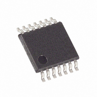
DS1845E-050+T&R Maxim Integrated Products, DS1845E-050+T&R Datasheet - Page 4

DS1845E-050+T&R
Manufacturer Part Number
DS1845E-050+T&R
Description
IC POT/MEM DUAL NV 50K 14-TSSOP
Manufacturer
Maxim Integrated Products
Datasheet
1.DS1845E-010.pdf
(14 pages)
Specifications of DS1845E-050+T&R
Taps
100, 256
Resistance (ohms)
10K, 50K
Number Of Circuits
2
Temperature Coefficient
750 ppm/°C Typical
Memory Type
Non-Volatile
Interface
I²C, 2-Wire Serial
Voltage - Supply
2.7 V ~ 5.5 V
Operating Temperature
-40°C ~ 85°C
Mounting Type
Surface Mount
Package / Case
14-TSSOP
Resistance In Ohms
10K and 50K
Lead Free Status / RoHS Status
Lead free / RoHS Compliant
DS1845
2-Wire Interface Reset: After any interruption in protocol, power loss, or system reset, the following
steps reset the DS1845.
1. Clock up to nine cycles.
2. Look for SDA high in each cycle while SCL is high.
3. Create a start condition while SDA is high.
Device Addressing: The DS1845 must receive an 8-bit device address word following a start condition
to enable a specific device for a read or write operation. The address word is clocked into the DS1845
MSB to LSB. The address word consists of Ah (1010) followed by A2, A1, and A0 then the R/W
(READ/WRITE) bit. If the R/W bit is high, a read operation is initiated. The R/W is low, a write
operation is initiated. For a device to become active, the values of A2, A1 and A0 must be the same as
the hard-wired address pins on the DS1845. Upon a match of written and hard-wired addresses, the
DS1845 will output a zero for one clock cycle as an acknowledge. If the address does not match the
DS1845 returns to a low-power mode.
Write Operations: After receiving a matching address byte with the R/W bit set low, the device goes
into the write mode of operation. The master must transmit an 8-bit EEPROM memory address to the
device to define the address where the data is to be written. After the reception of this byte, the DS1845
will transmit a zero for one clock cycle to acknowledge the receipt of the address. The master must then
transmit an 8-bit data word to be written into this address. The DS1845 will again transmit a zero for one
clock cycle to acknowledge the receipt of the data. At this point the master must terminate the write
operation with a stop condition. The DS1845 then enters an internally timed write process t
to the
w
EEPROM memory. All inputs are disabled during this byte write cycle.
The DS1845 is capable of an 8-byte page write. A page write is initiated the same way as a byte write,
st
but the master does not send a stop condition after the 1
byte. Instead, after the slave acknowledges
receipt of the data byte, the master can send up to seven more bytes using the same nine-clock sequence.
The master must terminate the write cycle with a stop condition or the data clocked into the DS1845 will
not be latched into permanent memory.
Acknowledge Polling: Once the internally-timed write has started and the DS1845 inputs are disabled,
acknowledge polling can be initiated. The process involves transmitting a start condition followed by the
device address. The R/W bit signifies the type of operation that is desired. The read or write sequence
will only be allowed to proceed if the internal write cycle has completed and the DS1845 responds with a
zero.
Read Operations: After receiving a matching address byte with the R/W bit set high, the device goes
into the read mode of operation. There are three read operations: current address read, random read and
sequential address read.
4 of 14


