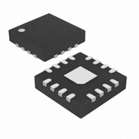
MAX5483ETE+T Maxim Integrated Products, MAX5483ETE+T Datasheet - Page 4

MAX5483ETE+T
Manufacturer Part Number
MAX5483ETE+T
Description
IC POT DGTL 10BIT NV 16-TQFN
Manufacturer
Maxim Integrated Products
Datasheet
1.MAX5481EUD.pdf
(20 pages)
Specifications of MAX5483ETE+T
Taps
1024
Resistance (ohms)
10K
Number Of Circuits
1
Temperature Coefficient
35 ppm/°C Typical
Memory Type
Non-Volatile
Interface
SPI, 3-Wire Serial
Voltage - Supply
2.7 V ~ 5.25 V, ±2.5 V ~ 5.25 V
Operating Temperature
-40°C ~ 85°C
Mounting Type
Surface Mount
Package / Case
16-TQFN Exposed Pad
Resistance In Ohms
10K
Lead Free Status / RoHS Status
Lead free / RoHS Compliant
10-Bit, Nonvolatile, Linear-Taper Digital
Potentiometers
TIMING CHARACTERISTICS
(V
V
4
Note 1: 100% production tested at T
Note 2: The DNL and INL are measured with the device configured as a voltage-divider with H = V
Note 3: The DNL_R and INL_R are measured with D.N.C. unconnected and L = V
Note 4: The wiper resistance is measured using the source currents given in Note 3.
Note 5: The device draws higher supply current when the digital inputs are driven with voltages between (V
Note 6: Wiper settling test condition uses the voltage-divider configuration with a 10pF load on W. Transition code from 00000 00000
ANALOG SECTION
Wiper Settling Time (Note 6)
SPI-COMPATIBLE SERIAL INTERFACE (Figure 3)
SCLK Frequency
SCLK Clock Period
SCLK Pulse-Width High
SCLK Pulse-Width Low
CS Fall to SCLK Rise Setup
SCLK Rise to CS Rise Hold
DIN to SCLK Setup
DIN Hold after SCLK
SCLK Rise to CS Fall Delay
CS Rise to SCLK Rise Hold
CS Pulse-Width High
Write NV Register Busy Time
UP/DOWN DIGITAL INTERFACE (Figure 8)
CS to INC Setup
INC High to U/D Change
U/D to INC Setup
INC Low Period
INC High Period
INC Inactive to CS Inactive
CS Deselect Time (Store)
INC Cycle Time
INC Active to CS Inactive
Wiper Store Cycle
DD
DD
_______________________________________________________________________________________
= +5.0V, T
= +2.7V to +5.25V, V
nal (W) is unloaded and measured with a high-input-impedance voltmeter.
ven with a source current of I
nal is driven with a source current of 40µA for the 50kΩ device and 200µA for the 10kΩ device.
0.5V). See Supply Current vs. Digital Input Voltage in the Typical Operating Characteristics .
to 01111 01111 and measure the time from CS going high to the wiper voltage settling to within 0.5% of its final value.
PARAMETER
A
= +25°C, unless otherwise noted.) (Note 1)
SS
= V
GND
A
SYMBOL
W
= 0V, V
= +25°C and T
f
t
t
t
t
t
t
= 80µA for the 50kΩ device and 400µA for the 10kΩ device. For V
SCLK
t
t
t
BUSY
CSW
WSC
t
CSH
t
CPH
CYC
t
t
CSS
t
CS0
CS1
t
t
t
t
t
t
CH
DH
t
CP
CL
DS
t
CI
ID
DI
IH
IC
IK
IL
S
H
= V
MAX5481
MAX5482
DD
A
, V
= +85°C. Guaranteed by design to T
L
= 0V, T
CONDITIONS
A
= -40°C to +85°C, unless otherwise noted. Typical values are at
SS
= 0V. For V
A
= -40°C.
DD
MIN
140
150
60
60
60
40
15
60
25
20
25
25
25
50
50
50
50
0
0
DD
= +5V, the wiper terminal is dri-
and L = V
DD
TYP
22
DD
5
= +3V, the wiper termi-
- 0.5V) and (V
SS
. The wiper termi-
MAX
12
12
7
GND
UNITS
MHz
ms
ms
µs
ns
ns
ns
ns
ns
ns
ns
ns
ns
ns
ns
ns
ns
ns
ns
ns
ns
ns
ns
+


