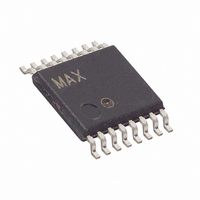
DS1856E-020+ Maxim Integrated Products, DS1856E-020+ Datasheet - Page 12

DS1856E-020+
Manufacturer Part Number
DS1856E-020+
Description
IC RES TEMP-CNTRL 20/20K 16TSSOP
Manufacturer
Maxim Integrated Products
Datasheet
1.DS1856B-050.pdf
(31 pages)
Specifications of DS1856E-020+
Taps
256
Resistance (ohms)
20K
Number Of Circuits
2
Temperature Coefficient
50 ppm/°C Typical
Memory Type
Non-Volatile
Interface
I²C, 2-Wire Serial
Voltage - Supply
2.85 V ~ 5.5 V
Operating Temperature
-40°C ~ 95°C
Mounting Type
Surface Mount
Package / Case
16-TSSOP
Resistance In Ohms
20K
Lead Free Status / RoHS Status
Lead free / RoHS Compliant
Dual, Temperature-Controlled Resistors with Inter-
nally Calibrated Monitors and Password Protection
memories can be accessed by two separate 2-wire
slave addresses (see Table 4). The Main Device
address is A2h (or determined by the value in Table 03,
byte 8Ch, when ADFIX = 1) and the Auxiliary Device
address is A0h (fixed). A configuration bit, ADEN
(Table 03, byte 89h, bit 5), determines whether the
DS1856 uses one or two 2-wire slave addresses. This
feature can be used to save component count in SFF
applications or other applications where both GBIC
and monitoring functions are implemented and two
device addresses are needed.
The memory organization for ADEN = 0 is shown in
Figure 2. In this configuration, the 128 bytes of
Auxiliary Device EEPROM are located at memory loca-
tions 00h to 7Fh and accessed using the Auxiliary
Device 2-wire slave address of A0h (fixed). The
remainder of the DS1856’s memory is accessed using
the Main Device address.
The memory organization of the second configuration,
ADEN = 1, is shown in Figure 3. In this configuration, all
12
Figure 3. Memory Organization, ADEN = 1
____________________________________________________________________
DEC HEX
0
200
127
128
183
199
255
0
C7
C8
7F
80
B7
FF
2-WIRE ADDRRESS A2h (DEFAULT)
00h
80h
TABLE SELECT BYTE
AUXILIARY MEMORY
PASSWORD ENTRY
LOWER MEMORY
(PWE) (4 BYTES)
TABLE 00h/01h
(128 BYTES)
EEPROM
FFh
7Fh
80h
CONFIGURATION
TABLE 03h
TABLE
NOTE 1: ADEN BIT = 1. ALL MEMORY (INCLUDING THE AUXILIARY MEMORY) IS ADDRESSED USING THE
NOTE 1:
NOTE 2: TABLES 00h AND 01h ACCESS THE SAME PHYSICAL MEMORY.
NOTE 3: TABLE 02h DOES NOT EXIST.
B7h
MAIN DEVICE 2-WIRE SLAVE ADDRESS.
of the DS1856’s memory including the Auxiliary memo-
ry is accessed using only the Main Device address.
The Auxiliary Device memory is mapped into Table 00
and Table 01 in the Main Device. Both tables map to
the same block of physical memory. This is done to
improve the compatibility between previous members
of this IC family such as the DS1858/DS1859 and the
DS1852. In this configuration, the DS1856 ignores com-
munication using the Auxiliary Device address.
The value of the Main Device address can be changed
to a value other than the default value of A2h (see data
sheet Table 5). There can be up to 128 devices sharing
a common 2-wire bus, with each device having its own
unique address. To change the Main Device address,
first write the desired value to the Chip Address byte
(Table 03, byte 8Ch). Then, enable the new address by
setting ADFIX to a 1. Subsequent 2-wire communica-
tion must be performed using the new Main Device
address. When ADFIX = 0, the Chip Address byte is
ignored, and the Main Device address is set to A2h.
80h
F0h
LOOK-UP TABLE
RESERVED AND
CALIBRATION
RESISTOR 0
CONSTANTS
TABLE 04h
(72 BYTES)
C7h
FFh
80h
F0h
LOOK-UP TABLE
RESERVED AND
CALIBRATION
RESISTOR 1
CONSTANTS
TABLE 05h
(72 BYTES)
C7h
FFh


