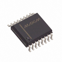
DS1868S-50+ Maxim Integrated Products, DS1868S-50+ Datasheet - Page 11

DS1868S-50+
Manufacturer Part Number
DS1868S-50+
Description
IC POT DIGITAL DUAL 50K 16-SOIC
Manufacturer
Maxim Integrated Products
Datasheet
1.DS1868-10.pdf
(14 pages)
Specifications of DS1868S-50+
Taps
256
Resistance (ohms)
50K
Number Of Circuits
2
Temperature Coefficient
750 ppm/°C Typical
Memory Type
Volatile
Interface
3-Wire Serial
Voltage - Supply
2.7 V ~ 3.3 V, 4.5 V ~ 5.5 V
Operating Temperature
-40°C ~ 85°C
Mounting Type
Surface Mount
Package / Case
16-SOIC (0.300", 7.5mm Width)
Resistance In Ohms
50K
Number Of Pots
Dual
Taps Per Pot
256
Resistance
50 KOhms
Wiper Memory
Volatile
Digital Interface
Serial (3-Wire)
Operating Supply Voltage
4.5 V to 5.5 V
Supply Current
1 uA
Maximum Operating Temperature
+ 85 C
Minimum Operating Temperature
- 40 C
Description/function
Dual Digital Potentiometer Chip
Mounting Style
SMD/SMT
Supply Voltage (max)
5.5 V
Supply Voltage (min)
4.5 V
Tolerance
20 %
Lead Free Status / RoHS Status
Lead free / RoHS Compliant
CAPACITANCE
AC ELECTRICAL CHARACTERISTICS
NOTES:
1. All voltages are referenced to ground.
2. Resistor inputs cannot exceed V
3. Capacitance values apply at 25 C.
4. Absolute linearity is used to determine wiper voltage versus expected voltage as determined by wiper
5. Relative linearity is used to determine the change in voltage between successive tap positions. Device
6. Typical values are for t
7. -3 dB cutoff frequency characteristics for the DS1868 depend on potentiometer total resistance:
8. Cout is active regardless of the state of
9. V
10. See Figure 9(a), (b), and (c).
11. Noise < -120 dB/
12. Supply current is dependent on clock rate (see Figure 11).
13. See Figure 10.
14. Standby currents apply when
15. When biasing the substrate minimum V
16. Valid at 25 C only.
PARAMETER
Input Capacitance
Output Capacitance
PARAMETER
CLK Frequency
Width of CLK Pulse
Data Setup Time
Data Hold Time
Propagation Delay Time Low to High Level
Clock to Output
Propagation Delay Time High to Low Level
Clock Low to Data Valid on a Read
CLK Rise Time, CLK Fall Time
RST
RST
RST
position. Device test limits 1.6 LSB.
test limits 0.5 LSB.
DS1868-010; 1 MHz, DS1868-050; 200 kHz; and DS1868-100; 80 kHz.
REF
High to Clock Input High
Low from Clock Input High
Inactive
= 1.5 volts.
Hz
. Reference 1 volt (thermal).
A
= 25 C and nominal supply voltage.
RST
B
- 0.5V in the negative direction.
, LLIC, DQ are in the low-state.
B
RST
= -3.0V
SYMBOL
SYMBOL
.
11 of 14
C
f
t
t
t
t
t
t
C
t
t
t
t
CDH
CDD
CLK
PLH
PLH
HLT
RLT
OUT
CH
DC
CC
CR
IN
10% and maximum V
(-40 C to +85 C; V
MIN
MIN
125
DC
50
30
10
50
50
TYP
TYP
CC
MAX UNITS
MAX UNITS
10
50
50
30
50
5
7
= 3.0V
CC
=5.0V
MHz
pF
pF
ns
ns
ns
ns
ns
ns
ns
ns
ns
ns
10%.
(t
A
=25 C)
NOTES
NOTES
10, 13
10, 13
10%)
DS1868
3, 6
3, 6
10
10
10
10
10
10
10
10
10


