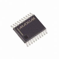
DS1267E-100 Maxim Integrated Products, DS1267E-100 Datasheet - Page 4

DS1267E-100
Manufacturer Part Number
DS1267E-100
Description
IC POT DUAL DIGITAL 100K 20TSSOP
Manufacturer
Maxim Integrated Products
Datasheet
1.DS1267-100.pdf
(12 pages)
Specifications of DS1267E-100
Taps
256
Resistance (ohms)
100K
Number Of Circuits
2
Temperature Coefficient
750 ppm/°C Typical
Memory Type
Volatile
Interface
3-Wire Serial
Voltage - Supply
4.5 V ~ 5.5 V
Operating Temperature
-40°C ~ 85°C
Mounting Type
Surface Mount
Package / Case
20-TSSOP
Resistance In Ohms
100K
Lead Free Status / RoHS Status
Contains lead / RoHS non-compliant
Other names
DS1267E100
Available stocks
Company
Part Number
Manufacturer
Quantity
Price
Part Number:
DS1267E-100
Manufacturer:
MAXIM/美信
Quantity:
20 000
Company:
Part Number:
DS1267E-100+
Manufacturer:
MAGNACHIP
Quantity:
24 000
Company:
Part Number:
DS1267E-100/T&R
Manufacturer:
MAXIM
Quantity:
2 944
Company:
Part Number:
DS1267E-100A2
Manufacturer:
MAXIM
Quantity:
2 944
DS1267
STACKED CONFIGURATION
The potentiometers of the DS1267 can be connected in series as shown in Figure 3. This is referred to as
the stacked configuration. The stacked configuration allows the user to double the total end-to-end
resistance of the part and the number of steps to 512 (or 9 bits of resolution).
The wiper output for the combined stacked potentiometer will be taken at the S
pin, which is the
OUT
multiplexed output of the wiper of potentiometer-0 (W0) or potentiometer-1 (W1). The potentiometer
wiper selected at the S
output is governed by the setting of the stack select bit (bit 0) of the 17-bit I/O
OUT
shift register. If the stack select bit has value 0, the multiplexed output, S
, will be that of the
OUT
potentiometer-0 wiper. If the stack select bit has value 1, the multiplexed output, S
, will be that of the
OUT
potentiometer-1 wiper.
STACKED CONFIGURATION Figure 3
CASCADE OPERATION
A feature of the DS1267 is the ability to control multiple devices from a single processor. Multiple
DS1267s can be linked or daisy-chained as shown in Figure 4. As a data bit is entered into the I/O shift
register of the DS1267 a bit will appear at the C
output within a maximum delay of 50 nanoseconds.
OUT
The stack select bit of the DS1267 will always be the first out the part at the beginning of a transaction.
Additionally the C
pin is always active regardless of the state of
. This allows one to read the I/O
RST
OUT
shift register without changing its value.
CASCADING MULTIPLE DEVICES Figure 4
4 of 12
102199


