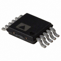
AD5201BRM10 Analog Devices Inc, AD5201BRM10 Datasheet - Page 13

AD5201BRM10
Manufacturer Part Number
AD5201BRM10
Description
IC DGTL POT 10K 33POS 10-MSOP
Manufacturer
Analog Devices Inc
Datasheet
1.AD5200BRMZ10.pdf
(16 pages)
Specifications of AD5201BRM10
Rohs Status
RoHS non-compliant
Taps
33
Resistance (ohms)
10K
Number Of Circuits
1
Temperature Coefficient
500 ppm/°C Typical
Memory Type
Volatile
Interface
SPI, 3-Wire Serial
Voltage - Supply
2.7 V ~ 5.5 V, ±2.3 V ~ 2.7 V
Operating Temperature
-40°C ~ 85°C
Mounting Type
Surface Mount
Package / Case
10-MSOP, Micro10™, 10-uMAX, 10-uSOP
Resistance In Ohms
10K
D
(DEC)
255
128
1
0
D
(DEC)
32
16
1
0
The tolerance of the nominal resistance can be ± 30% due to
process lot dependance. If users apply the RDAC in rheostat
(variable resistance) mode, they should be aware of such specifi-
cation of tolerance. The change in R
500 ppm/°C temperature coefficient.
PROGRAMMING THE POTENTIOMETER DIVIDER
Voltage Output Operation
The digital potentiometer easily generates output voltages at
wiper-to-B and wiper-to-A to be proportional to the input volt-
age at A to B.
Unlike the polarity of V
age across A–B, W–A, and W–B can be at either polarity.
If ignoring the effects of the wiper resistance for an approxima-
tion, connecting A terminal to 5 V and B terminal to ground
produces an output voltage at the wiper which can be any value
starting at almost zero to almost full scale with the minor devia-
tion contributed by the wiper resistance. Each LSB of voltage is
equal to the voltage applied across Terminal AB divided by the
2
AD5200 and AD5201 respectively. The general equation defin-
ing the output voltage with respect to ground for any valid input
voltage applied to Terminals A and B is:
where D in AD5200 is between 0 to 255 and D in AD5201 is
between 0 to 32.
For more accurate calculation, including the effects of wiper
resistance, V
where R
1 to 4.
N
-1 and 2
V
V
V
W
W
W
( )
( )
( )
WB
D
D
D
N
(D) and R
=
=
=
position resolution of the potentiometer divider for
W
255
R
32
can be found as:
D
D
AD5200 Wiper-to-A Resistance
AD5201 Wiper-to-A Resistance
WB
R
R
( )
50
5030
10011
10050
R
( )
50
5050
9738
10050
V
AB
( )
V
WA
WA
D
AB
AB
WA
+
DD
V
+
(D) can be obtained from Equations
A
V
V
– V
B
+
B
R
SS
WA
R
, which must be positive, volt-
AB
for AD5201
( )
for AD5200
D
AB
V
Output State
Full-Scale (R
Midscale
1 LSB
Zero-Scale (R
Output State
Full-Scale (R
Midscale
1 LSB
Zero-Scale (R
with temperature has a
B
W
W
AB
AB
)
)
+ R
+ R
W
W
)
)
(5)
(6)
(7)
Operation of the digital potentiometer in the divider mode results
in more accurate operation over temperature. Here the output
voltage is dependent on the ratio of the internal resistors and not
the absolute values; therefore, the drift reduces to 15 ppm/°C.
DIGITAL INTERFACING
The AD5200/AD5201 contain a standard three-wire serial input
control interface. The three inputs are clock (CLK), CS, and
serial data input (SDI). The positive-edge-sensitive CLK input
requires clean transitions to avoid clocking incorrect data into
the serial input register. Standard logic families work well. If
mechanical switches are used for product evaluation, they
should be debounced by a flip-flop or other suitable means.
Figure 3 shows more detail of the internal digital circuitry. When
CS is low, the clock loads data into the serial register on each
positive clock edge (see Table III).
CLK CS
L
P
X
X
X
NOTE
P = positive edge, X = don’t care, SR = shift register.
All digital inputs are protected with a series input resistor and
parallel Zener ESD structure shown in Figure 4. Applies to
digital input pins CS, SDI, SHDN, CLK.
GND
CLK
L
L
P
H
H
V
SDI
CS
DD
Table III. Input Logic Control Truth Table
SHDN
H
H
H
H
L
PWR-ON
PRESET
AD5200/AD5201
REG
Register Activity
No SR effect.
Shift one bit in from the SDI pin.
Load SR data into RDAC latch.
No operation.
Open circuit on A terminal and short
circuit between W to B terminals.
SER
340
Dx
A,B,W
V
8/6
SS
V
SS
AD5200/AD5201
RDAC
LOGIC
REG
V
A
W
B
SHDN
SS


