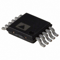
AD5201BRM10 Analog Devices Inc, AD5201BRM10 Datasheet - Page 4

AD5201BRM10
Manufacturer Part Number
AD5201BRM10
Description
IC DGTL POT 10K 33POS 10-MSOP
Manufacturer
Analog Devices Inc
Datasheet
1.AD5200BRMZ10.pdf
(16 pages)
Specifications of AD5201BRM10
Rohs Status
RoHS non-compliant
Taps
33
Resistance (ohms)
10K
Number Of Circuits
1
Temperature Coefficient
500 ppm/°C Typical
Memory Type
Volatile
Interface
SPI, 3-Wire Serial
Voltage - Supply
2.7 V ~ 5.5 V, ±2.3 V ~ 2.7 V
Operating Temperature
-40°C ~ 85°C
Mounting Type
Surface Mount
Package / Case
10-MSOP, Micro10™, 10-uMAX, 10-uSOP
Resistance In Ohms
10K
AD5200/AD5201–SPECIFICATIONS
ELECTRICAL CHARACTERISTICS
Parameter
INTERFACE TIMING CHARACTERISTICS (Applies to All Parts [Notes 2, 3])
NOTES
1
2
3
Specifications subject to change without notice.
Typicals represent average readings at 25°C and V
Guaranteed by design and not subject to production test.
See timing diagram for location of measured values. All input control voltages are specified with t
1.5 V. Switching characteristics are measured using V
Input Clock Pulsewidth
Data Setup Time
Data Hold Time
CS Setup Time
CS High Pulsewidth
CLK Fall to CS Fall Hold Time
CLK Fall to CS Rise Hold Time
CS Rise to Clock Rise Setup
(DATA IN)
VOUT
VOUT
VOUT
CLK
CLK
SDI
CLK
CS
SDI
SDI
DD
CS
CS
V
Symbol
t
t
t
t
t
t
t
t
CH
DS
DH
CSS
CSW
CSH0
CSH1
CS1
DD
= 5 V, V
LOGIC
1
0
1
0
1
0
0
1
0
1
0
1
0
1
0
1
0
1
0
1
0
1
0
, t
t
CL
CSH0
= 5 V.
(V
unless otherwise noted.)
SS
t
DD
CSS
Dx
= 0 V.
D7
= 5 V
D5
Conditions
Clock Level High or Low
t
D6
CH
D4
DAC REGISTER LOAD
DAC REGISTER LOAD
10%, or 3 V
D5
t
DS
Dx
t
CL
D4
D3
D3
D2
t
DH
D2
10%, V
t
CSH1
R
D1
= t
D1
F
t
SS
CS1
= 2 ns (10% to 90% of 3 V) and timed from a voltage level of
D0
= 0 V, V
D0
t
CSW
t
S
Min
20
5
5
15
40
0
0
10
1LSB
A
= +V
DD
, V
B
Typ
= 0 V, –40 C < T
1
Max
A
< +85 C
Unit
ns
ns
ns
ns
ns
ns
ns
ns


