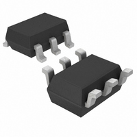
LTC2630ISC6-LZ12#TRMPBF Linear Technology, LTC2630ISC6-LZ12#TRMPBF Datasheet

LTC2630ISC6-LZ12#TRMPBF
Specifications of LTC2630ISC6-LZ12#TRMPBF
Available stocks
Related parts for LTC2630ISC6-LZ12#TRMPBF
LTC2630ISC6-LZ12#TRMPBF Summary of contents
Page 1
... The LTC2630 incorporates a power-on reset circuit. Options are available for reset to zero or reset to mid-scale after power-up LTC and LTM are registered trademarks of Linear Technology Corporation. All other trademarks are the property of their respective owners. Protected by U.S. Patents including 5396245, 5859606, 6891433, 6937178 and 7414561 ...
Page 2
LTC2630 ABSOLUTE MAXIMUM RATINGS (Notes 1, 2) Supply Voltage (V ) ................................... –0. CS/LD, SCK, SDI .......................................... –0. ..................................–0.3V to min(V OUT Operating Temperature Range LTC2630C ................................................ 0°C to 70°C LTC2630I..............................................–40°C to 85°C LTC2630H ...
Page 3
PRODUCT SELECTION GUIDE PART NUMBER PART MARKING* V WITH INTERNAL REFERENCE FS LTC2630A-LM12 LCZB LTC2630A-LZ12 LCSB LTC2630A-HM12 LCWR LTC2630A-HZ12 LCZC LTC2630-LM12 LCZB LTC2630-LM10 LCZF LTC2630-LM8 LCYW LTC2630-LZ12 LCSB LTC2630-LZ10 LCZD LTC2630-LZ8 LCYV LTC2630-HM12 LCWR LTC2630-HM10 LCZH LTC2630-HM8 LCYY LTC2630-HZ12 LCZC ...
Page 4
LTC2630 ELECTRICAL CHARACTERISTICS temperature range, otherwise specifi cations are at T LTC2630-LM12/-LM10/-LM8/-LZ12/-LZ10/-LZ8, LTC2630A-LM12/-LZ12 (V SYMBOL PARAMETER CONDITIONS DC Performance Resolution Monotonicity V = 3V, Internal Ref. (Note 4) CC DNL Differential Nonlinearity V = 3V, Internal Ref. (Note 4) CC ...
Page 5
ELECTRICAL CHARACTERISTICS temperature range, otherwise specifi cations are at T LTC2630-LM12/-LM10/-LM8/-LZ12/-LZ10/-LZ8, LTC2630A-LM12/-LZ12 (V SYMBOL PARAMETER AC Performance t Settling Time S Voltage Output Slew Rate Capacitive Load Driving Glitch Impulse e Output Voltage Noise Density n Output Voltage Noise TIMING ...
Page 6
LTC2630 ELECTRICAL CHARACTERISTICS temperature range, otherwise specifi cations are at T LTC2630-HM12/-HM10/-HM8/-HZ12/-HZ10/-HZ8, LTC2630A-HM12/-HZ12 (V SYMBOL PARAMETER CONDITIONS DC Performance Resolution Monotonicity V = 5V, Internal Ref. (Note 4) CC DNL Differential Nonlinearity V = 5V, Internal Ref. (Note 4) CC ...
Page 7
ELECTRICAL CHARACTERISTICS temperature range, otherwise specifi cations are at T LTC2630-HM12/-HM10/-HM8/-HZ12/-HZ10/-HZ8, LTC2630A-HM12/-HZ12 (V SYMBOL PARAMETER AC Performance t Settling Time S Voltage Output Slew Rate Capacitive Load Driving Glitch Impulse e Output Voltage Noise Density n Output Voltage Noise TIMING ...
Page 8
LTC2630 TYPICAL PERFORMANCE CHARACTERISTICS LTC2630-LM12/-LZ12 (V = 2.5V) FS Integral Nonlinearity (INL) 1 0.5 0 –0.5 –1.0 2048 0 1024 CODE INL vs Temperature 1 0.5 INL (POS) 0 INL (NEG) –0.5 ...
Page 9
TYPICAL PERFORMANCE CHARACTERISTICS LTC2630-HM12/-HZ12 (V = 4.096V) FS Integral Nonlinearity (INL) 1 0.5 0 –0.5 –1.0 2048 0 1024 CODE INL vs Temperature 1 0.5 INL (POS) 0 INL (NEG) –0.5 –1.0 ...
Page 10
LTC2630 TYPICAL PERFORMANCE CHARACTERISTICS LTC2630-10 Integral Nonlinearity (INL) 1 4.096V FS 0.5 0 –0.5 –1.0 512 0 256 CODE LTC2630-8 Integral Nonlinearity (INL) 1 2.5V FS 0.5 0 ...
Page 11
TYPICAL PERFORMANCE CHARACTERISTICS LTC2630 Large-Signal Response 0.5V/DIV 1/4 SCALE TO 3/4 SCALE 2μs/DIV 2630 G22 Headroom at Rails vs Output Current 5.0 5V SOURCING 4.5 4.0 3.5 3V (LTC2630-L) SOURCING 3.0 2.5 2.0 ...
Page 12
LTC2630 PIN FUNCTIONS CS/LD (Pin 1): Serial Interface Chip Select/Load Input. When CS/LD is low, SCK is enabled for shifting data on SDI into the register. When CS/LD is taken high, SCK is disabled and the specifi ed command (see ...
Page 13
TIMING DIAGRAM SCK SDI CS/LD OPERATION The LTC2630 is a family of single voltage output DACs in 6-lead SC70 packages. Each DAC can operate rail-to-rail referenced to the input supply, or with its full-scale voltage set ...
Page 14
LTC2630 OPERATION INPUT WORD (LTC2630-12) COMMAND 4 DON'T-CARE BITS INPUT WORD (LTC2630-10) COMMAND 4 DON'T-CARE BITS INPUT WORD (LTC2630-8) COMMAND 4 DON'T-CARE BITS Serial Interface ...
Page 15
OPERATION The 16-bit data word is ignored for all commands that do not include a Write operation. Power-Down Mode For power-constrained applications, power-down mode can be used to reduce the supply current whenever the DAC output is not needed. When ...
Page 16
LTC2630 OPERATION Rail-to-Rail Output Considerations In any rail-to-rail voltage output device, the output is limited to voltages within the supply range. Since the analog output of the DAC cannot go below ground, it may limit for the lowest codes as ...
Page 17
OPERATION Optoisolated 4mA to 20mA Process Controller Figure 5 shows how to use an LTC2630HZ to make an optoisolated, digitally-controlled 4mA to 20mA transmitter. The transmitter circuitry, including optoisolation, is powered by the loop voltage which has a wide range ...
Page 18
LTC2630 OPERATION 18 2630fe ...
Page 19
... JEDEC PACKAGE REFERENCE IS MO-203 VARIATION AB Information furnished by Linear Technology Corporation is believed to be accurate and reliable. However, no responsibility is assumed for its use. Linear Technology Corporation makes no representa- tion that the interconnection of its circuits as described herein will not infringe on existing patent rights. 2.7V TO 5.5V 0.1μ ...
Page 20
... OUT Selectable External Ref. Mode, Rail-to-Rail Output, SPI Interface www.linear.com ● V LOOP 5.4V TO 80V + 1k Q1 LTC2054 2N3440 – 1000 F P 10k R S 10Ω I OUT 2630 TA02 2 C Interface 2 C Interface LT 1108 REV E • PRINTED IN USA © LINEAR TECHNOLOGY CORPORATION 2007 2630fe ...


