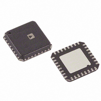
AD9704BCPZ Analog Devices Inc, AD9704BCPZ Datasheet - Page 13

AD9704BCPZ
Manufacturer Part Number
AD9704BCPZ
Description
IC DAC TX 8BIT 175MSPS 32-LFCSP
Manufacturer
Analog Devices Inc
Series
TxDAC®r
Datasheet
1.AD9704BCPZ.pdf
(52 pages)
Specifications of AD9704BCPZ
Data Interface
Serial
Settling Time
11ns
Number Of Bits
8
Number Of Converters
1
Voltage Supply Source
Analog and Digital
Power Dissipation (max)
50mW
Operating Temperature
-40°C ~ 85°C
Mounting Type
Surface Mount
Package / Case
32-LFCSP
Resolution (bits)
8bit
Sampling Rate
175MSPS
Input Channel Type
Parallel
Supply Current
5.1mA
Digital Ic Case Style
CSP
No. Of Pins
32
Supply Voltage Range - Analogue
3.3V To 3.6V
Rohs Compliant
Yes
Number Of Channels
1
Resolution
8b
Interface Type
Parallel
Single Supply Voltage (typ)
1.8/3.3V
Architecture
Segment
Power Supply Requirement
Analog and Digital
Output Type
Current
Integral Nonlinearity Error
±0.09LSB
Single Supply Voltage (min)
1.7V
Single Supply Voltage (max)
3.6V
Operating Temp Range
-40C to 85C
Operating Temperature Classification
Industrial
Mounting
Surface Mount
Pin Count
32
Package Type
LFCSP EP
Lead Free Status / RoHS Status
Lead free / RoHS Compliant
Lead Free Status / RoHS Status
Lead free / RoHS Compliant, Lead free / RoHS Compliant
Available stocks
Company
Part Number
Manufacturer
Quantity
Price
Company:
Part Number:
AD9704BCPZ
Manufacturer:
Analog Devices Inc
Quantity:
135
Company:
Part Number:
AD9704BCPZ
Manufacturer:
FREESCAL
Quantity:
2
Part Number:
AD9704BCPZ
Manufacturer:
ADI/亚德诺
Quantity:
20 000
AD9705
Table 11. AD9705 Pin Function Descriptions
Pin No.
27
28 to 32,
1, 2, 4
5
25
24
23
22
21
20
19
18
17
16
15
14
13
12
11
10, 26
6 to 9
3
Mnemonic
DB9 (MSB)
DB8 to DB1
DB0 (LSB)
SLEEP/CSB
FS ADJ
REFIO
ACOM
IOUTA
IOUTB
OTCM
AVDD
PIN/SPI/RESET
MODE/SDIO
CMODE/SCLK
CLKCOM
CLK−
CLK+
CLKVDD
DCOM
NC
DVDD
Description
Most Significant Data Bit (MSB).
Least Significant Data Bit (LSB).
In pin mode, active high powers down chip.
In SPI mode, this pin is the serial port chip select (active low).
Full-Scale Current Output Adjust.
Reference Input/Output. Serves as reference input when internal reference disabled. Serves as 1.0 V reference
output when internal reference is activated. Requires a 0.1 μF capacitor to ACOM when internal reference is activated.
Analog Common.
DAC Current Output. Full-scale current is sourced when all data bits are 1s.
Complementary DAC Current Output. Full-scale current is sourced when all data bits are 0s.
Adjustable Output Common Mode. Refer to the Theory of Operation section for details.
Analog Supply Voltage (1.7 V to 3.6 V).
Selects SPI mode or pin mode operation. Active high for pin mode operation. Active low for SPI mode
operation. Pulse high to reset SPI registers to default values.
In pin mode, this selects the input data format. Connect to DCOM for straight binary, DVDD for twos complement.
In SPI mode, this pin acts as SPI data input/output.
In pin mode, this pin selects the clock input type. Connect to CLKCOM for single-ended clock receiver
(drive CLK+ and float CLK–). Connect to CLKVDD for differential receiver.
In SPI mode, this pin is the serial data clock input.
Clock Common.
Negative Differential Clock Input.
Positive Differential Clock Input.
Clock Supply Voltage (1.7 V to 3.6 V).
Digital Common.
No Connect.
Digital Supply Voltage (1.7 V to 3.6 V).
Data Bit 8 to Data Bit 1.
DB0 (LSB)
DVDD
NC = NO CONNECT
DB3
DB2
DB1
NC
NC
NC
Figure 5. AD9705 Pin Configuration
1
2
3
4
5
6
7
8
Rev. A | Page 13 of 52
(Not to Scale)
PIN 1
INDICATOR
AD9705
TOP VIEW
24
23
22
21
20
19
18
17
FS ADJ
REFIO
ACOM
IOUTA
IOUTB
OTCM
AVDD
PIN/SPI/RESET
AD9704/AD9705/AD9706/AD9707


