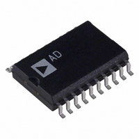
AD7849BRZ Analog Devices Inc, AD7849BRZ Datasheet - Page 4

AD7849BRZ
Manufacturer Part Number
AD7849BRZ
Description
IC DAC 14/16BIT SRL-IN 20-SOIC
Manufacturer
Analog Devices Inc
Datasheet
1.AD7849BRZ.pdf
(20 pages)
Specifications of AD7849BRZ
Data Interface
Serial
Settling Time
7µs
Number Of Bits
16
Number Of Converters
1
Voltage Supply Source
Analog and Digital, Dual ±
Power Dissipation (max)
100mW
Operating Temperature
-40°C ~ 85°C
Mounting Type
Surface Mount
Package / Case
20-SOIC (7.5mm Width)
Resolution (bits)
16bit
Sampling Rate
143kSPS
Input Channel Type
Serial
Supply Voltage Range - Digital
4.75V To 5.25V
Supply Current
5mA
Digital Ic Case Style
SOIC
Lead Free Status / RoHS Status
Lead free / RoHS Compliant
Available stocks
Company
Part Number
Manufacturer
Quantity
Price
Company:
Part Number:
AD7849BRZ
Manufacturer:
ADI
Quantity:
429
Part Number:
AD7849BRZ
Manufacturer:
ADI/亚德诺
Quantity:
20 000
Parameter
DIGITAL INPUTS
DIGITAL OUTPUTS
POWER REQUIREMENTS
1
2
3
RESET SPECIFICATIONS
These specifications apply when the device goes into reset mode during power-up or power-down sequence. V
Table 2.
Parameter
V
V
V
V
G2 R
1
AD7849
Guaranteed by design and characterization, not production tested.
The AD7849 is functional with power supplies of ±12 V. See the Typical Performance Characteristics section.
Sensitivity of gain error, offset error, and bipolar zero error to V
A pull-down resistor (65 kΩ) on V
A
B
C
D
,
, High Threshold Voltage for V
, Low Threshold Voltage for V
Input High Voltage, V
Input Low Voltage, V
Input Current, I
Input Capacitance, C
Output Low Voltage, V
Output High Voltage, V
Floating State Leakage Current
Floating State Output
V
V
V
I
I
I
Power Supply Sensitivity
Power Dissipation
, High Threshold Voltage for V
1
DD
SS
CC
DD
SS
CC
Low Threshold Voltage for V
ON
Capacitance
INH
INL
IN
INH
2
OL
OH
3
OUT
CC
maintains 0 V output when V
DD
CC
DD
, V
, V
SS
SS
A Version
2.4
0.8
±10
10
0.4
4.0
±10
10
14.25/15.75
−14.25/−15.75
4.75/5.25
5
5
2.5
0.4
100
All Versions
1.2
0
9.5
6.4
1
0
4
2.5
1
DD
B Version
2.4
0.8
±10
10
0.4
4.0
±10
10
14.25/15.75
−14.25/−15.75
4.75/5.25
5
5
2.5
1.5
100
, V
DD
SS
/V
variations.
SS
Unit
V max
V typ
V max
V min
V max
V typ
V max
V min
kΩ typ
is below V
Rev. C | Page 4 of 20
This is the higher V
Below this, the reset is activated. Typically, 8 V.
Below this, the reset is activated. Typically, 3 V.
Test Conditions/Comments
This is the lower V
Above this, the reset is activated.
This is the lower V
Above this, the reset is activated.
This is the higher V
On resistance of G2; V
A
.
C Version
2.4
0.8
±10
10
0.4
4.0
±10
10
14.25/15.75
−14.25/−15.75
4.75/5.25
5
5
2.5
1.5
100
DD
CC
Unit
V min
V max
μA max
pF max
V max
V min
μA max
pF max
V min/V max
V min/V max
V min/V max
mA max
mA max
mA max
LSB/V max
mW typ
DD
CC
/V
threshold voltage for the reset function.
/V
threshold voltage for the reset function.
DD
SS
SS
threshold voltage for the reset function.
= 2 V; V
threshold voltage for the reset function.
SS
= −2 V; I
Test Conditions/Comments
I
I
V
V
V
V
V
V
SINK
SOURCE
OUT
INL
OUT
INL
INH
OUT
= 0.1 V
= 0.1 V
= 1.6 mA
= V
unloaded, V
unloaded, V
unloaded
= 400 μA
G2
DD
OUT
= 1 mA.
– 0.1 V, V
unloaded.
INH
INH
INL
= V
= V
= 0.1 V
DD
DD
– 0.1 V,
– 0.1 V,


