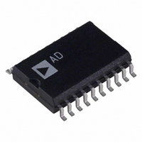
AD7849BRZ Analog Devices Inc, AD7849BRZ Datasheet

AD7849BRZ
Specifications of AD7849BRZ
Available stocks
Related parts for AD7849BRZ
AD7849BRZ Summary of contents
Page 1
FEATURES 14-bit/16-bit multiplying DAC Guaranteed monotonicity Output control on power-up and power-down internal or external control Versatile serial interface DAC clears both unipolar and bipolar output ranges APPLICATIONS Industrial process controls PC analog I/O boards Instrumentation ...
Page 2
AD7849 TABLE OF CONTENTS Features .............................................................................................. 1 Applications....................................................................................... 1 Functional Block Diagram .............................................................. 1 General Description ......................................................................... 1 Revision History ............................................................................... 2 Specifications..................................................................................... 3 Reset Specifications ...................................................................... 4 AC Performance Characteristics ................................................ 5 Timing Characteristics ................................................................ 5 Absolute Maximum Ratings............................................................ ...
Page 3
SPECIFICATIONS V = 14. 15. −14. −15. connected unless otherwise noted. Temperature range for versions is −40°C ...
Page 4
AD7849 Parameter A Version DIGITAL INPUTS Input High Voltage, V 2.4 INH Input Low Voltage, V 0.8 INL Input Current, I ±10 INH Input Capacitance DIGITAL OUTPUTS Output Low Voltage, V 0.4 OL Output High Voltage, V ...
Page 5
AC PERFORMANCE CHARACTERISTICS These characteristics are included for design guidance and are no subject to test. V −15 connected OFS Table 3. Parameter DYNAMIC PERFORMANCE 1 Output ...
Page 6
AD7849 ABSOLUTE MAXIMUM RATINGS T = 25°C, unless otherwise noted. A Table 5. Parameter V to DGND DGND DGND DGND REF DGND REF− DGND OUT ...
Page 7
PIN CONFIGURATION AND FUNCTION DESCRIPTIONS Table 6. Pin Function Descriptions Pin No. Mnemonic Description Input. The DAC is specified for V REF+ REF Input. The DAC is specified for V REF− REF− ...
Page 8
AD7849 TYPICAL PERFORMANCE CHARACTERISTICS V 1 REF OUT CH1 1.00V M 20.0µs CH1 CH4 1.00mV Figure 3. AC Feedthrough SYNC 1 SDIN OUT CH2 5.00V M 1.00µs CH1 5.00V CH4 200mV Figure 4. Digital-to-Analog Glitch ...
Page 9
V REF OUT CH1 100mV CH2 200mV M 2.00µs CH1 Figure 9. Pulse Response (Small Signal) 2 25° REF REF– GAIN = 1 1.5 1.0 0.5 0 11.00 ...
Page 10
AD7849 TERMINOLOGY Least Significant Bit This is the analog weighting of 1 bit of the digital word in a DAC. For the B version and the C versions, 1 LSB = ( )/2 . For the A version, ...
Page 11
CIRCUIT DESCRIPTION DIGITAL-TO-ANALOG CONVERSION Figure 15 shows the digital-to-analog section of the AD7849. There are three on-chip DACs, each of which has its own buffer amplifier. DAC1 and DAC2 are 4-bit DACs. They share a 16-resistor string, but they have ...
Page 12
AD7849 SCLK SYNC BIN/COMP SDIN DB15 (AD7849B/C) SDIN DB13 (AD7849A) LDAC, CLR NOTES 1. DCEN IS TIED PERMANENTLY LOW. DIGITAL INTERFACE The AD7849 contains an input serial-to-parallel shift register and a DAC latch. A simplified diagram of the input loading ...
Page 13
SCLK t 2 SYNC BIN/COMP SDIN DB15 (N) (AD7849B/C) SDOUT (AD7849B/C) SDIN DB13 (N) DB0 (N) (AD7849A) SDOUT (AD7849A) LDAC, CLR NOTES 1. DCEN IS TIED PERMANENTLY HIGH. Serial Data Loading Format (Daisy-Chain Mode) By connecting DCEN high, daisy-chain mode ...
Page 14
AD7849 Unipolar Configuration Figure 20 shows the AD7849 in the unipolar binary circuit configuration. The DAC is driven by the AD586 reference. Because R is tied the output amplifier has a gain of ×2, OFS ...
Page 15
Other Output Voltage Ranges In some cases, users may require output voltage ranges other than those already mentioned. One example is systems that need the output voltage whole number of millivolts (that is mV). ...
Page 16
AD7849 AD7849-to-TMS320C2x Interface Figure 25 shows a serial interface between the AD7849 and the TMS320C2x DSP processor. In this interface, the CLKX and FSX signals for the TMS320C2x should be generated using external clock/timer circuitry. The FSX pin of the ...
Page 17
APPLICATIONS INFORMATION OPTO-ISOLATED INTERFACE In many process control applications necessary to provide an isolation barrier between the controller and the unit being controlled. Opto-isolators can provide voltage isolation in excess of 3 kV. The serial loading structure of ...
Page 18
AD7849 OUTLINE DIMENSIONS 0.210 (5.33) MAX 0.150 (3.81) 0.130 (3.30) 0.115 (2.92) 0.022 (0.56) 0.018 (0.46) 0.014 (0.36) 0.30 (0.0118) 0.10 (0.0039) COPLANARITY 0.10 1.060 (26.92) 1.030 (26.16) 0.980 (24.89 0.280 (7.11) 0.250 (6.35) 1 0.240 (6.10) 10 ...
Page 19
... AD7849ARZ-REEL −40°C to +85°C AD7849BR −40°C to +85°C AD7849BR-REEL −40°C to +85°C AD7849BRZ −40°C to +85°C AD7849BRZ-REEL −40°C to +85°C AD7849CR −40°C to +85°C AD7849CR-REEL −40°C to +85°C AD7849CRZ −40°C to +85°C AD7849CRZ-REEL − ...
Page 20
AD7849 NOTES ©1995–2011 Analog Devices, Inc. All rights reserved. Trademarks and registered trademarks are the property of their respective owners. D01008-0-3/11(C) Rev Page ...


