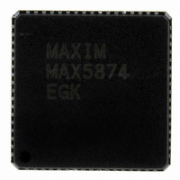
MAX5874EGK+D Maxim Integrated Products, MAX5874EGK+D Datasheet - Page 10

MAX5874EGK+D
Manufacturer Part Number
MAX5874EGK+D
Description
IC DAC 14BIT 200MSPS DUAL 68-QFN
Manufacturer
Maxim Integrated Products
Datasheet
1.MAX5874EGKD.pdf
(16 pages)
Specifications of MAX5874EGK+D
Settling Time
14ns
Number Of Bits
14
Data Interface
Parallel
Number Of Converters
2
Voltage Supply Source
Analog and Digital
Power Dissipation (max)
300mW
Operating Temperature
-40°C ~ 85°C
Mounting Type
Surface Mount
Package / Case
68-QFN Exposed Pad
Lead Free Status / RoHS Status
Lead free / RoHS Compliant
14-Bit, 200Msps, High-Dynamic-Performance,
Dual DAC with CMOS Inputs
Figure 1. MAX5874 High-Performance, 14-Bit, Dual Current-Steering DAC
Each MAX5874 DAC outputs two complementary cur-
rents (OUTIP/N, OUTQP/N) that operate in a single-
ended or differential configuration. A load resistor
converts these two output currents into complementary
single-ended output voltages. A transformer or a differ-
ential amplifier configuration converts the differential
voltage existing between OUTIP (OUTQP) and OUTIN
(OUTQN) to a single-ended voltage. If not using a
transformer, the recommended termination from the
output is a 25Ω termination resistor to ground and a
50Ω resistor between the outputs.
To generate a single-ended output, select OUTIP (or
OUTQP) as the output and connect OUTIN (or OUTQN)
to GND. SFDR degrades with single-ended operation.
Figure 3 displays a simplified diagram of the internal
output structure of the MAX5874.
The MAX5874 features flexible differential clock inputs
(CLKP, CLKN) operating from a separate supply
10
______________________________________________________________________________________
DATA13–
DATA0
(OUTIP, OUTIN, OUTQP, OUTQN)
SELIQ
AV
TORB
CLKP
CLKN
DORI
GND
XOR
CLK
Clock Inputs (CLKP, CLKN)
RECEIVER
DV
CMOS
DD3.3
GND
LATCH
Analog Outputs
INTERFACE
POWER-DOWN
CLK
BLOCK
DV
PD
DD1.8
LATCH
LATCH
AV
DD1.8
DECODE
DECODE
(AV
Drive the differential clock inputs from a single-ended
or a differential clock source. For single-ended opera-
tion, drive CLKP with a logic source and bypass CLKN
to GND with a 0.1µF capacitor.
CLKP and CLKN are internally biased to AV
facilitates the AC-coupling of clock sources directly to
the device without external resistors to define the DC
level. The dynamic input resistance from CLKP and
CLKN to ground is > 5kΩ.
Figure 4 displays the timing relationship between digital
CMOS data, clock, and output signals. The MAX5874
features a 1.5ns hold, a -1.2ns setup, and a 1.1ns propa-
gation delay time. A nine (eight)-clock-cycle latency
exists between CLKP/CLKN and OUTIP/OUTIN
(OUTQP/OUTQN) when operating in single-port (inter-
leaved) mode. In dual-port (parallel) mode, the clock
latency is 5.5 clock cycles for both channels. Table 2
shows the DAC output codes.
XOR/
XOR/
CLK
) to achieve the optimum jitter performance.
LATCH
LATCH
MAX5874
GND
AV
DD3.3
Data Timing Relationship
LATCH
LATCH
REFERENCE
1.2V
DAC
DAC
DACREF
OUTQP
OUTQN
FSADJ
OUTIP
OUTIN
REFIO
CLK
/ 2. This


