MAX5888AEGK+D Maxim Integrated Products, MAX5888AEGK+D Datasheet
MAX5888AEGK+D
Specifications of MAX5888AEGK+D


Related parts for MAX5888AEGK+D


MAX5888AEGK+D Summary of contents
Page 1
... Communications: LMDS, MMDS, Point-to-Point Microwave Digital Signal Synthesis Automated Test Equipment (ATE) Instrumentation ________________________________________________________________ Maxim Integrated Products For pricing, delivery, and ordering information, please contact Maxim/Dallas Direct! at 1-888-629-4642, or visit Maxim’s website at www.maxim-ic.com. o 500Msps Output Update Rate o Single 3.3V Supply Operation ...
Page 2
High Dynamic Performance DAC with Differential LVDS Inputs ABSOLUTE MAXIMUM RATINGS VCLK to AGND................................-0.3V to +3. VCLK to DGND ...............................-0.3V to +3. ...
Page 3
High Dynamic Performance DAC with Differential LVDS Inputs ELECTRICAL CHARACTERISTICS (continued) ( VCLK = 3.3V, AGND = DGND = CLKGND = 0, external reference analog output, 50Ω double terminated (Figure 7), ...
Page 4
High Dynamic Performance DAC with Differential LVDS Inputs ELECTRICAL CHARACTERISTICS (continued) ( VCLK = 3.3V, AGND = DGND = CLKGND = 0, external reference analog output, 50Ω double terminated (Figure 7), ...
Page 5
High Dynamic Performance DAC with Differential LVDS Inputs ELECTRICAL CHARACTERISTICS (continued) ( VCLK = 3.3V, AGND = DGND = CLKGND = 0, external reference analog output, 50Ω double terminated (Figure 7), ...
Page 6
High Dynamic Performance DAC with Differential LVDS Inputs ( VCLK = 3.3V, external reference SFDR vs. OUTPUT FREQUENCY (f = 200MHz -6dB FS) CLK OUT 100 I = 20mA ...
Page 7
High Dynamic Performance DAC with Differential LVDS Inputs PIN NAME 1 B3P Data Bit 3 2 B3N Complementary Data Bit 3 3 B2P Data Bit 2 4 B2N Complementary Data Bit 2 5 B1P Data Bit 1 ...
Page 8
High Dynamic Performance DAC with Differential LVDS Inputs PIN NAME 45 B14N Complementary Data Bit 14 46 B13P Data Bit 13 47 B13N Complementary Data Bit 13 48 B12P Data Bit 12 49 B12N Complementary Data Bit ...
Page 9
High Dynamic Performance DAC with Differential LVDS Inputs DV DD 1.2V REFERENCE REFIO REFADJ CLKN CLKP Figure 1. Simplified MAX5888 Block Diagram Table 1. I and R Selection Matrix Based on a Typical 1.200V Reference Voltage OUT ...
Page 10
High Dynamic Performance DAC with Differential LVDS Inputs 1.2V REFERENCE 10kΩ REFIO 0.1µF FSADJ CURRENT-STEERING I REF R SET DACREF REF REFIO SET Figure 2. Reference Architecture, Internal Reference Configuration operation IOUTP should ...
Page 11
High Dynamic Performance DAC with Differential LVDS Inputs DIGITAL DATA IS LATCHED ON THE RISING EDGE OF CLKP B0 TO B15 SETUP CLKP CLKN IOUT Figure 5. Detailed Timing Relationship ...
Page 12
High Dynamic Performance DAC with Differential LVDS Inputs AV DD B0–B15 16 AGND Figure 7. Differential to Single-Ended Conversion Using a Wideband RF Transformer AV DV VCLK DD DD IOUTP B0–B15 MAX5888 IOUTN 16 AGND DGND CLKGND ...
Page 13
High Dynamic Performance DAC with Differential LVDS Inputs carriers spread their IM products over a bandwidth of 20MHz on either side of the 20MHz total carrier band- width. In this four-carrier scenario, only the energy in the ...
Page 14
High Dynamic Performance DAC with Differential LVDS Inputs The number of carriers and their signal levels with respect to the full scale of the DAC are important as well. Unlike a full-scale sine wave, the inherent nature ...
Page 15
High Dynamic Performance DAC with Differential LVDS Inputs O MEASUREMENT BANDWIDTH -30 30kHz 100kHz -60 -70 -73 -75 -80 -90 0.2 0.4 0.6 1.2 1.8 FREQUENCY OFFSET FROM CARRIER (MHz) Figure 11. GSM/EDGE Tx Mask Grounding, Bypassing, ...
Page 16
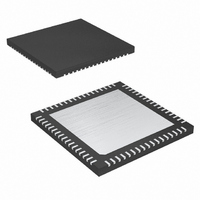
High Dynamic Performance DAC with Differential LVDS Inputs The MAX5888 is packaged in a 68-lead QFN-EP package (package code: G6800-4), providing greater design flexibility, increased thermal efficiency**, and optimized AC performance of the DAC. The exposed pad ...
Page 17
High Dynamic Performance DAC with Differential LVDS Inputs The offset error is the difference between the ideal and the actual offset current. For a DAC, the offset point is the value at the output for the two ...
Page 18
... Maxim reserves the right to change the circuitry and specifications without notice at any time. implied. Maxim reserves the right to change the circuitry and specifications without notice at any time. 18 ____________________Maxim Integrated Products, 120 San Gabriel Drive, Sunnyvale, CA 94086 408-737-7600 18 ____________________Maxim Integrated Products, 120 San Gabriel Drive, Sunnyvale, CA 94086 408-737-7600 © ...