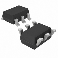
LTC2630ISC6-LM8#TRMPBF Linear Technology, LTC2630ISC6-LM8#TRMPBF Datasheet - Page 15

LTC2630ISC6-LM8#TRMPBF
Manufacturer Part Number
LTC2630ISC6-LM8#TRMPBF
Description
IC DAC 8BIT R-R SC70-6
Manufacturer
Linear Technology
Datasheet
1.LTC2630CSC6-LZ8TRMPBF.pdf
(20 pages)
Specifications of LTC2630ISC6-LM8#TRMPBF
Settling Time
3.2µs
Number Of Bits
8
Data Interface
Serial
Number Of Converters
1
Voltage Supply Source
Single Supply
Power Dissipation (max)
480µW
Operating Temperature
-40°C ~ 85°C
Mounting Type
Surface Mount
Package / Case
SC-70-6, SC-88, SOT-363
Lead Free Status / RoHS Status
Lead free / RoHS Compliant
Available stocks
Company
Part Number
Manufacturer
Quantity
Price
OPERATION
The 16-bit data word is ignored for all commands that do
not include a Write operation.
Power-Down Mode
For power-constrained applications, power-down mode
can be used to reduce the supply current whenever the
DAC output is not needed. When in power-down, the buffer
amplifi er, bias circuit, and reference circuit are disabled
and draw essentially zero current. The DAC output is put
into a high-impedance state, and the output pin is passively
pulled to ground through a 200kΩ resistor. Input and DAC
register contents are not disturbed during power-down.
The DAC can be put into power-down mode by using
command 0100. The supply current is reduced to 1.8μA
maximum when the DAC is powered down.
Normal operation resumes after executing any command
that includes a DAC update, as shown in Table 1. The DAC
is powered up and its voltage output is updated. Normal
settling is delayed while the bias, reference, and amplifi er
circuits are re-enabled. The power-up delay time is 18μs
for settling to 12-bits.
Reference Modes
For applications where an accurate external reference is
not available, the LTC2630 has a user-selectable, integrated
reference. The LTC2630-LM and LTC2630-LZ provide a full-
scale output of 2.5V. The LTC2630-HM and LTC2630-HZ
provide a full-scale output of 4.096V.
The internal reference can be useful in applications where
the supply voltage is poorly regulated. Internal Reference
mode can be selected by using command 0110, and is
the power-on default.
The DAC can also operate in supply as reference mode us-
ing command 0111. In this mode, V
reference voltage and the supply current is reduced.
Voltage Output
The LTC2630’s integrated rail-to-rail amplifier has
guaranteed load regulation when sourcing or sinking up
to 10mA at 5V, and 5mA at 3V.
Load regulation is a measure of the amplifi er’s ability to
maintain the rated voltage accuracy over a wide range of
load current. The measured change in output voltage per
change in forced load current is expressed in LSB/mA.
DC output impedance is equivalent to load regulation, and
may be derived from it by simply calculating a change in
units from LSB/mA to ohms. The amplifi er’s DC output
impedance is 0.1Ω when driving a load well away from
the rails.
When drawing a load current from either rail, the output
voltage headroom with respect to that rail is limited by
the 50Ω typical channel resistance of the output devices
(e.g., when sinking 1mA, the minimum output voltage is
50Ω • 1mA, or 50mV). See the graph “Headroom at Rails
vs. Output Current” in the Typical Performance Charac-
teristics section.
The amplifi er is stable driving capacitive loads of up to
500pF.
CC
supplies the DAC’s
LTC2630
15
2630fe


