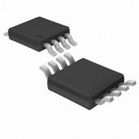
LTC1663CMS8 Linear Technology, LTC1663CMS8 Datasheet - Page 7

LTC1663CMS8
Manufacturer Part Number
LTC1663CMS8
Description
IC DAC 10BIT R-R MICROPWR 8MSOP
Manufacturer
Linear Technology
Datasheet
1.LTC1663CS5TRMPBF.pdf
(12 pages)
Specifications of LTC1663CMS8
Settling Time
30µs
Number Of Bits
10
Data Interface
Serial
Number Of Converters
1
Voltage Supply Source
Single Supply
Power Dissipation (max)
630µW
Operating Temperature
0°C ~ 70°C
Mounting Type
Surface Mount
Package / Case
8-MSOP, Micro8™, 8-uMAX, 8-uSOP,
Lead Free Status / RoHS Status
Contains lead / RoHS non-compliant
Available stocks
Company
Part Number
Manufacturer
Quantity
Price
Company:
Part Number:
LTC1663CMS8
Manufacturer:
LT
Quantity:
10 000
Part Number:
LTC1663CMS8
Manufacturer:
LINEAR/凌特
Quantity:
20 000
Company:
Part Number:
LTC1663CMS8#TRPBF
Manufacturer:
LINEAR
Quantity:
11 123
DEFINITIONS
Integral Nonlinearity (INL): The deviation from a straight
line passing through the endpoints of the DAC transfer
curve (Endpoint INL). Because the output cannot go
below zero, the linearity is measured between full scale
and the lowest code that guarantees the output will be
greater than zero. The INL error at a given input code is
calculated as follows:
Where V
at the given input code.
Least Signifi cant Bit (LSB): The ideal voltage difference
between two successive codes.
APPLICATIONS INFORMATION
Serial Digital Interface
The LTC1663 communicates with a host (master) using
the standard 2-wire interface. The Timing Diagram shows
the timing relationship of the signals on the bus. The two
bus lines, SDA and SCL, must be high when the bus is
not in use. External pull-up resistors or current sources,
such as the LTC1694 SMBus Accelerator, are required on
these lines.
The LTC1663 is a receive-only (slave) device. The master
can communicate with the LTC1663 using the Quick Com-
mand, Send Byte or Write Word protocols as explained
later.
The START and STOP Conditions
When the bus is not in use, both SCL and SDA must be
high. A bus master signals the beginning of a communica-
tion to a slave device by transmitting a START condition.
A START condition is generated by transitioning SDA
from high to low while SCL is high.
INL = [V
LSB = V
OUT
REF
OUT
is the output voltage of the DAC measured
/1024
– V
OS
– (V
S = Start Condition, Wr = Write Bit = 0, A = Acknowledge, P = Stop Condition
1
S
FS
– V
Slave Address
OS
7
)(code/1023)]/LSB
Wr
1
Write Word Protocol Used by the LTC1663
1
A
Command Byte
8
A
1
Resolution (n): Defi nes the number of DAC output states
(2
imply linearity.
Voltage Offset Error (V
output when the DAC is loaded with all zeros. A single
supply DAC can have a true negative offset, but the output
cannot go below zero (see Applications Information).
For this reason, single supply DAC offset is measured at
the lowest code that guarantees the output will be greater
than zero.
When the master has fi nished communicating with the
slave, it issues a STOP condition. A STOP condition is
generated by transitioning SDA from low to high while
SCL is high. The bus is then free for communication with
another SMBus device.
Acknowledge
The Acknowledge signal is used for handshaking between
the master and the slave. An Acknowledge (active LOW)
generated by the slave lets the master know that the latest
byte of information was received. The Acknowledge related
clock pulse is generated by the master. The master releases
the SDA line (HIGH) during the Acknowledge clock pulse.
The slave-receiver must pull down the SDA line during the
Acknowledge clock pulse so that it remains a stable LOW
during the HIGH period of this clock pulse.
Write Word Protocol
The master initiates communication with the LTC1663 with
a START condition and a 7-bit address followed by the Write
LSData Byte
n
) that divide the full-scale range. Resolution does not
8
1
A
MSData Byte
8
OS
): Nominally, the voltage at the
A
1
1663 TA03
1
P
LTC1663
1663fd
7


