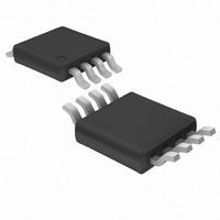
LTC1663CMS8 Linear Technology, LTC1663CMS8 Datasheet - Page 9

LTC1663CMS8
Manufacturer Part Number
LTC1663CMS8
Description
IC DAC 10BIT R-R MICROPWR 8MSOP
Manufacturer
Linear Technology
Datasheet
1.LTC1663CS5TRMPBF.pdf
(12 pages)
Specifications of LTC1663CMS8
Settling Time
30µs
Number Of Bits
10
Data Interface
Serial
Number Of Converters
1
Voltage Supply Source
Single Supply
Power Dissipation (max)
630µW
Operating Temperature
0°C ~ 70°C
Mounting Type
Surface Mount
Package / Case
8-MSOP, Micro8™, 8-uMAX, 8-uSOP,
Lead Free Status / RoHS Status
Contains lead / RoHS non-compliant
Available stocks
Company
Part Number
Manufacturer
Quantity
Price
Company:
Part Number:
LTC1663CMS8
Manufacturer:
LT
Quantity:
10 000
Part Number:
LTC1663CMS8
Manufacturer:
LINEAR/凌特
Quantity:
20 000
Company:
Part Number:
LTC1663CMS8#TRPBF
Manufacturer:
LINEAR
Quantity:
11 123
APPLICATIONS INFORMATION
Data Bytes
Least Signifi cant Data Byte
Most Signifi cant Data Byte
X = Don’t care
Send Byte Protocol
The Send Byte protocol used on the LTC1663 is actually a
subset of the Write Word protocol described previously.
The Send Byte protocol can only be used to send the
command byte information to the LTC1663.
The Send Byte protocol is also used whenever the Write
Word protocol is interrupted for any reason. Reception of
a START or STOP condition after the Acknowledge of the
command byte, but before the Acknowledge of the last
data byte, will cause both data bytes to be ignored and
the command byte to be accepted.
Reception of a START or STOP condition before the Ac-
knowledge of the command byte will cause the interrupted
command byte to be ignored.
SYNC Address/Quick Command
In addition to the slave address, the LTC1663 has an address
that can be shared by other devices so that they may be
updated synchronously. The address is called to the SYNC
address and uses the quick command protocol.
The SYNC Address is 1111 110
SY/CLR
D7
7
7
X
S = Start Condition, Wr = Write Bit, A = Acknowledge, P = Stop Condition
1
S
1
0
D6
6
X
6
Slave Address
Update output latches on rising edge of SCL during
Acknowledge of SYNC Address
Clear all internal latches on rising edge of SCL during
Acknowledge of SYNC Address
Start
1
7
SYNC Address
D5
5
X
5
1111 110
7
Wr
1
4
X
D4
4
SY/CLR
1
A
1
Command Byte
3
X
D3
3
8
Ack
1
X
2
D2
2
Stop
1663 TA05
1
1
A
P
1
D9
D1
1
1
1663 TA04
D0
D8
0
0
The SY/CLR bit set high only has meaning when the “SY”
bit of the command byte was previously set HIGH. On
the otherhand, the SY/CLR bit set LOW will always clear
the part, independent of the state of the “SY” bit in the
command byte.
Input Threshold
Anticipating the trend toward lower supply voltages,
the SMBus is specifi ed with a V
0.6V. While some SMBus parts may violate this stringent
SMBus specifi cation by allowing a higher V
correspondingly higher input supply voltage, the LTC1663
meets and maintains the constant SMBus input threshold
specifi cation across the entire supply voltage range of
2.7V to 5.5V. The logic input threshold is designed to be
1V with 50mV of hysteresis.
Voltage Output
The output amplifi er contained in the LTC1663 can source
or sink up to 5mA. The output stage swings to within a
few millivolts of either supply rail when unloaded and
has an equivalent output resistance of 85Ω when driving
a load to the rails. The output amplifi er is stable driving
capacitive loads up to 1000pF .
A small resistor placed in series with the output can be
used to achieve stability for any load capacitance greater
than 1000pF . For example, a 0.1μF load can be driven
by the LTC1663 if a 110Ω series resistance is used. The
phase margin of the resulting circuit is 45° and increases
monotonically from this point if larger values of resistance,
capacitance or both are substituted for the values given.
Rail-to-Rail Output Considerations
As in any rail-to-rail device, the output is limited to volt-
ages within the supply range.
If the DAC offset is negative, the output for the lowest
codes limits at 0V as shown in Figure 1b.
Similarly, limiting can occur near full scale when V
used as the reference. If V
error (FSE) is positive, the output for the highest codes
limits at V
can occur if the internal reference is used.
CC
as shown in Figure 1c. No full-scale limiting
REF
= V
CC
IH
and the DAC full-scale
of 1.4V and a V
LTC1663
IH
value for a
CC
IL
1663fd
9
of
is


