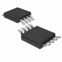
LTC1661IMS8 Linear Technology, LTC1661IMS8 Datasheet

LTC1661IMS8
Specifications of LTC1661IMS8
Available stocks
Related parts for LTC1661IMS8
LTC1661IMS8 Summary of contents
Page 1
... Digitally Controlled Amplifiers and Attenuators n Portable Battery-Powered Instruments n Automatic Calibration for Manufacturing n Remote Industrial Devices n L, LT, LTC, LTM, Linear Technology and the Linear logo are registered trademarks of Linear Technology Corporation. All other trademarks are the property of their respective owners. BLOCK DIAGRAM V GND OUT ...
Page 2
... JA ORDER INFORMATION LEAD FREE FINISH TAPE AND REEL LTC1661CMS8#PBF LTC1661CMS8#TRPBF LTC1661IMS8#PBF LTC1661IMS8#TRPBF LTC1661CN8#PBF LTC1661CN8#TRPBF LTC1661IN8#PBF LTC1661IN8#TRPBF Consult LTC Marketing for parts specified with wider operating temperature ranges. Consult LTC Marketing for information on non-standard lead based finish parts. For more information on lead free part marking, go to: ...
Page 3
ELECTRICAL CHARACTERISTICS temperature range, otherwise specifications are at T SYMBOL PARAMETER Reference Input Input Voltage Range Resistance Capacitance I Reference Current REF Power Supply Positive Supply Voltage Supply Current CC DC Performance Short-Circuit Current Low Short-Circuit Current ...
Page 4
LTC1661 TIMING CHARACTERISTICS range, otherwise specifications are at T SYMBOL PARAMETER V = 2. Valid to SCK Setup Valid to SCK Hold SCK High Time 3 t SCK ...
Page 5
TYPICAL PERFORMANCE CHARACTERISTICS Integral Nonlinearity (INL) 2.0 1.5 1.0 0.5 0 –0.5 –1.0 –1.5 –2.0 0 256 512 768 CODE 1661 G01 Minimum V vs Load Current OUT (Output Sinking) 1400 1200 CODE = 0 125°C ...
Page 6
LTC1661 TYPICAL PERFORMANCE CHARACTERISTICS Supply Current vs Logic Input Voltage 1.0 0.8 0.6 0.4 0 LOGIC INPUT VOLTAGE (V) PIN FUNCTIONS CS/LD (Pin 1): Serial Interface Chip Select/Load Input. When CS/LD is low, SCK is enabled ...
Page 7
DEFINITIONS Differential Nonlinearity (DNL): The difference between the measured change and the ideal 1LSB change for any two adjacent codes. The DNL error between any two codes is calculated as follows: ∆V – LSB OUT DNL = LSB where ∆V ...
Page 8
LTC1661 OPERATION Transfer Function The transfer function for the LTC1661 is: k OUT(DEAL) REF 1024 where k is the decimal equivalent of the binary DAC input code D9-D0 and V is ...
Page 9
OPERATION Table 2. DAC Control Functions CONTROL INPUT REGISTER STATUS Change Load DAC Load DAC ...
Page 10
LTC1661 OPERATION Voltage Outputs Each of the rail-to-rail output amplifiers contained in the LTC1661 can typically source or sink up to 5mA (V The outputs swing to within a few millivolts of either supply when unloaded and have an equivalent ...
Page 11
TYPICAL APPLICATIONS 5V 0.1µ DAC A 1 CS/LD LTC1661 SCK DAC B 5V 0.1µ DAC B 1 LTC1661 DAC A 7 Figure 3. Pin Driver V V LTC1258-4.1 ...
Page 12
LTC1661 PACKAGE DESCRIPTION 5.23 (.206) MIN 0.42 ± 0.038 (.0165 ± .0015) TYP RECOMMENDED SOLDER PAD LAYOUT 0.254 (.010) GAUGE PLANE 0.18 (.007) NOTE: 1. DIMENSIONS IN MILLIMETER/(INCH) 2. DRAWING NOT TO SCALE 3. DIMENSION DOES NOT INCLUDE MOLD FLASH, ...
Page 13
... Removed typical values from Timing Characteristics section Information furnished by Linear Technology Corporation is believed to be accurate and reliable. However, no responsibility is assumed for its use. Linear Technology Corporation makes no representa- tion that the interconnection of its circuits as described herein will not infringe on existing patent rights. ...
Page 14
... OUT = 2.7V to 5.5V 2.5V CC OUT = 4.5V to 5.5V 4.095V CC OUT = 2.7V to 5.5V 2.5V CC OUT DAC. Output Swings from GND to OUT CC = 2.7V to 5.5V, Internal Reference, 60µA = 2.7V to 5.5V, Micropower, Rail-to-Rail Output LT 1110 REV A • PRINTED IN USA LINEAR TECHNOLOGY CORPORA TION 1999 CC 1661fa ...


