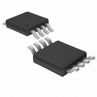
LTC1661IMS8 Linear Technology, LTC1661IMS8 Datasheet - Page 8

LTC1661IMS8
Manufacturer Part Number
LTC1661IMS8
Description
IC D/A CONV 10BIT MICRPWR 8-MSOP
Manufacturer
Linear Technology
Datasheet
1.LTC1661CMS8PBF.pdf
(14 pages)
Specifications of LTC1661IMS8
Settling Time
30µs
Number Of Bits
10
Data Interface
Serial
Number Of Converters
2
Voltage Supply Source
Single Supply
Power Dissipation (max)
260µW
Operating Temperature
-40°C ~ 85°C
Mounting Type
Surface Mount
Package / Case
8-MSOP, Micro8™, 8-uMAX, 8-uSOP,
Lead Free Status / RoHS Status
Contains lead / RoHS non-compliant
Available stocks
Company
Part Number
Manufacturer
Quantity
Price
Company:
Part Number:
LTC1661IMS8
Manufacturer:
LT
Quantity:
10 000
Part Number:
LTC1661IMS8
Manufacturer:
LT/凌特
Quantity:
20 000
Company:
Part Number:
LTC1661IMS8#TRPBF
Manufacturer:
LINEAR
Quantity:
10 169
Part Number:
LTC1661IMS8#TRPBF
Manufacturer:
LT
Quantity:
20 000
OPERATION
LTC1661
Transfer Function
The transfer function for the LTC1661 is:
where k is the decimal equivalent of the binary DAC input
code D9-D0 and V
Power-On Reset
The LTC1661 positively clears the outputs to zero scale
when power is first applied, making system initialization
consistent and repeatable.
Power Supply Sequencing
The voltage at REF (Pin 4) must not ever exceed the
voltage at V
should be taken in the power supply turn-on and turn-
off sequences to assure that this limit is observed. See
Absolute Maximum Ratings.
Serial Interface
See Table 1. The 16-bit Input word consists of the 4-bit
Control code, the 10-bit Input code and two don’t-care bits.
Table 1. LTC1661 Input Word
After the Input word is loaded into the register (see
Figure 1), it is internally converted from serial to parallel
format. The parallel 10-bit-wide input code data path is
then buffered by two latch registers.
The first of these, the input register, is used for loading
new input codes. The second buffer, the DAC register, is
used for updating the DAC outputs. Each DAC has its own
10-bit input register and 10-bit DAC register.
8
CONTROL CODE
A3 A2 A1
V
OUT(DEAL)
A0 D9 D8 D7 D6 D5 D4 D3 D2 D1
CC
=
(Pin 6) by more than 0.3V. Particular care
1024
REF
k
is the voltage at REF (Pin 6).
INPUT WORD
V
REF
INPUT CODE
D0
X1 X0
DON’T
CARE
By selecting the appropriate 4-bit control code (see Table 2)
it is possible to perform single operations, such as loading
one DAC or changing power-down status (sleep/wake).
In addition, some Control codes perform two or more
operations at the same time. For example, one such code
loads DAC A, updates both outputs and wakes the part
up. The DACs can be loaded separately or together, but
the outputs are always updated together.
Register Loading Sequence
See Figure 1. With CS/LD held low, data on the D
is shifted into the 16-bit shift register on the positive edge
of SCK. The 4-bit control code, A3-A0, is loaded first, then
the 10-bit Input code, D9-D0, ordered MSB-to-LSB in each
case. Two don’t-care bits, X1 and X0, are loaded last. When
the full 16-bit Input word has been shifted in, CS/LD is
pulled high, causing the system to respond according to
Table 2. The clock is disabled internally when CS/LD is
high. Note: SCK must be low when CS/LD is pulled low.
Sleep Mode
DAC control code 1110
instruction (see Table 2). In this mode, the digital parts
of the circuit stay active while the analog sections are
disabled; static power consumption is greatly reduced.
The reference input and analog outputs are set in a high
impedance state and all DAC settings are retained in
memory so that when Sleep mode is exited, the outputs
of DACs not updated by the wake command are restored
to their last active state.
Sleep mode is initiated by performing a load sequence
using control code 1110
ignored).
To save instruction cycles, the DACs may be prepared
with new input codes during Sleep (control codes 0001
and 0010
both to wake the part and to update the output values.
b
); then, a single command (1000
b
b
is reserved for the special sleep
(the DAC input code D9-D0 is
b
) can be used
IN
input
1661fa
b


