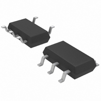
LTC1669-1CS5#TRMPBF Linear Technology, LTC1669-1CS5#TRMPBF Datasheet - Page 4

LTC1669-1CS5#TRMPBF
Manufacturer Part Number
LTC1669-1CS5#TRMPBF
Description
IC DAC 10BIT R-R I2C TSOT23-5
Manufacturer
Linear Technology
Datasheet
1.LTC1669CMS8PBF.pdf
(16 pages)
Specifications of LTC1669-1CS5#TRMPBF
Settling Time
30µs
Number Of Bits
10
Data Interface
I²C
Number Of Converters
1
Voltage Supply Source
Single Supply
Power Dissipation (max)
630µW
Operating Temperature
0°C ~ 70°C
Mounting Type
Surface Mount
Package / Case
TSOT-23-5, TSOT-5, TSOP-5
Number Of Channels
1
Resolution
10b
Interface Type
Serial (2-Wire/I2C)
Single Supply Voltage (typ)
3.3/5V
Dual Supply Voltage (typ)
Not RequiredV
Power Supply Requirement
Single
Output Type
Voltage
Integral Nonlinearity Error
±2.5LSB
Single Supply Voltage (min)
2.7V
Single Supply Voltage (max)
5.5V
Dual Supply Voltage (min)
Not RequiredV
Dual Supply Voltage (max)
Not RequiredV
Operating Temp Range
0C to 70C
Operating Temperature Classification
Commercial
Mounting
Surface Mount
Pin Count
5
Package Type
TSOT-23
Lead Free Status / RoHS Status
Lead free / RoHS Compliant
Other names
LTC1669-1CS5#PBF
LTC1669-1CS5#PBF
LTC1669-1CS5#PBF
Available stocks
Company
Part Number
Manufacturer
Quantity
Price
ELECTRICAL CHARACTERISTICS
LTC1669
ture range, otherwise specifi cations are at T
SYMBOL
Address Inputs AD0, AD1, AD2 (MSOP Only)
I
V
V
TIMING CHARACTERISTICS
range, otherwise specifi cations are at T
Note 1: Stresses beyond those listed under Absolute Maximum Ratings
may cause permanent damage to the device. Exposure to any Absolute
Maximum Rating condition for extended periods may affect device
reliability and lifetime.
Note 2: Nonlinearity and monotonicity are defi ned from code 20 to code
1003 (full scale). See Applications Information.
SYMBOL
Timing Characteristics (Notes 6, 7)
f
t
t
t
t
t
t
t
t
t
t
t
4
UP
SCL
BUF
HD, STA
SU, STA
SU, STO
HD, DAT (IN)
HD, DAT (OUT)
SU, DAT
LOW
HIGH
f
r
IH
IL
PARAMETER
Address Pin Pull-Up Current
High Level Input Voltage
Low Level Input Voltage
PARAMETER
Clock Operating Frequency
Bus Free Time Between Stop and Start Condition
Hold Time After (Repeated) Start Condition
Repeated Start Condition Setup Time
Stop Condition Setup Time
Data Hold Time (Input)
Data Hold Time (Output)
Data Setup Time
Clock Low Period
Clock High Period
Clock, Data Fall Time
Clock, Data Rise Time
A
= 25°C. V
A
= 25°C. V
CONDITIONS
V
IN
CC
The
= 0V
= 2.7V to 5.5V, V
CC
●
= 2.7V to 5.5V, V
denotes specifi cations which apply over the full operating temperature
The
●
denotes specifi cations which apply over the full operating tempera-
Note 3: Digital inputs at 0V or V
Note 4: Load is 10kΩ in parallel with 100pF .
Note 5: V
i.e., codes k = 102 and k = 922.
Note 6: All values are referenced to V
Note 7: Guaranteed by design and not subject to test.
CC
set as reference, V
CC
set as reference, V
CC
= V
REF
●
●
●
●
●
●
●
●
●
●
●
●
= 5V. DAC switched between 0.1V
l
l
l
OUT
MIN
225
250
4.7
4.7
4.7
20
20
4
4
0
4
V
unloaded, unless otherwise noted.
OUT
CC
CC
MIN
– 0.3
.
unloaded, unless otherwise noted.
IH
and V
TYP
500
TYP
0.5
IL
levels.
3450
1000
MAX
FS
100
300
and 0.9V
MAX
1.5
0.8
FS
,
UNITS
UNITS
1669fa
kHz
μA
μs
μs
μs
μs
ns
ns
ns
μs
μs
ns
ns
V
V


