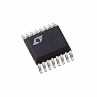
LTC2604IGN#TR Linear Technology, LTC2604IGN#TR Datasheet

LTC2604IGN#TR
Specifications of LTC2604IGN#TR
Available stocks
Related parts for LTC2604IGN#TR
LTC2604IGN#TR Summary of contents
Page 1
... The power-on reset circuit resets the LTC2604-1/LTC2614-1 /LTC2624-1 to midscale. The voltage outputs stay at mid- scale until a valid write and update take place. L, LT, LTC and LTM are registered trademarks of Linear Technology Corporation. All other trademarks are the property of their respective owners ...
Page 2
... LTC2624I-1 ..........................................–40°C to 85°C Storage Temperature Range .................. –65°C to 150°C Lead Temperature (Soldering, 10 sec)................... 300°C ORDER INFORMATION LEAD FREE FINISH TAPE AND REEL LTC2604CGN#PBF LTC2604CGN#TRPBF LTC2604CGN-1#PBF LTC2604CGN-1#TRPBF LTC2604IGN#PBF LTC2604IGN#TRPBF LTC2604IGN-1#PBF LTC2604IGN-1#TRPBF LTC2614CGN#PBF LTC2614CGN#TRPBF LTC2614CGN-1#PBF LTC2614CGN-1#TRPBF LTC2614IGN#PBF LTC2614IGN#TRPBF LTC2614IGN-1#PBF LTC2614IGN-1#TRPBF ...
Page 3
ELECTRICAL CHARACTERISTICS temperature range, otherwise specifi cations are at T REF C = REF D = 2.048V (V = 2.5V), REF SYMBOL PARAMETER CONDITIONS Load Regulation REF 0mA to ...
Page 4
LTC2604/LTC2614/LTC2624 ELECTRICAL CHARACTERISTICS temperature range, otherwise specifi cations are at T REF C = REF D = 2.048V (V = 2.5V), REF SYMBOL PARAMETER V Digital Input Low Voltage IL V Digital Output High Voltage ...
Page 5
TIMING CHARACTERISTICS range, otherwise specifi cations are 2.048V (V = 2.5V), REF OUT SYMBOL PARAMETER CS/LD High to SCK Positive Edge t 10 SCK Frequency Note 1: Stresses beyond those listed ...
Page 6
LTC2604/LTC2614/LTC2624 TYPICAL PERFORMANCE CHARATERISTICS (LTC2604/LTC2604-1, LTC2614/LTC2614-1, LTC2624/LTC2624-1) Gain Error 0.4 0.3 0.2 0.1 0 –0.1 –0.2 –0.3 –0.4 2.5 3 3 (V) CC 2604 G07 Midscale Glitch Impulse V OUT 10mV/DIV 12nV-s TYP ...
Page 7
TYPICAL PERFORMANCE CHARATERISTICS (LTC2604/LTC2604-1, LTC2614/LTC2614-1, LTC2624/LTC2624-1) Hardware CLR V OUT 1V/DIV CLR 5V/DIV 2604 G15 1μs/DIV Output Voltage Noise, 0.1Hz to 10Hz V OUT 10μV/DIV SECONDS 2604 G17 (LTC2604/LTC2604-1) Integral ...
Page 8
LTC2604/LTC2614/LTC2624 TYPICAL PERFORMANCE CHARATERISTICS (LTC2604/LTC2604-1) DNL vs Temperature 1 0 4.096V REF 0.6 0.4 DNL (POS) 0.2 0 –0.2 DNL (NEG) –0.4 –0.6 –0.8 –1.0 –50 –30 – TEMPERATURE (°C) ...
Page 9
TYPICAL PERFORMANCE CHARATERISTICS (LTC2624/LTC2624-1) Integral Nonlinearity (INL) 2 4.096V REF 1.5 1.0 0.5 0 –0.5 –1.0 –1.5 –2.0 0 1024 2048 3072 4095 CODE 2604 G31 PIN FUNCTIONS GND (Pin 1): Analog Ground. REF ...
Page 10
LTC2604/LTC2614/LTC2624 BLOCK DIAGRAM GND 1 REF LO 2 REF OUTA DAC OUTB DAC B 5 REF B 6 CS/LD 7 SCK 8 TIMING DIAGRAM SCK SDI CS/LD SDO OPERATION Power-On ...
Page 11
OPERATION Power Supply Sequencing The voltage at REF (Pins and 15) should be kept within the range – 0.3V ≤ REF x ≤ V lute Maximum Ratings). Particular care should be taken to observe these limits during ...
Page 12
LTC2604/LTC2614/LTC2624 OPERATION operation copies the data word from the input register to the DAC register. Once copied into the DAC register, the data word becomes the active 16-, 14- or 12-bit input code, and is converted to an analog voltage ...
Page 13
OPERATION LTC2604/LTC2614/LTC2624 2604fd 13 ...
Page 14
LTC2604/LTC2614/LTC2624 OPERATION DC output impedance is equivalent to load regulation, and may be derived from it by simply calculating a change in units from LSB/mA to Ohms. The amplifi ers’ DC output impedance is 0.025Ω when driving a load well ...
Page 15
... FLASH SHALL NOT EXCEED 0.010" (0.254mm) PER SIDE Information furnished by Linear Technology Corporation is believed to be accurate and reliable. However, no responsibility is assumed for its use. Linear Technology Corporation makes no representa- tion that the interconnection of its circuits as described herein will not infringe on existing patent rights. ...
Page 16
... OUT V = 2.7V to 5.5V, Micropower, Rail-to-Rail Output CC Precision 16-Bit Settling in 2μs for 10V Step 250μA per DAC, 2.5V to 5.5V Supply Range 300μA per DAC, 2.5V to 5.5V Supply Range LT 0309 REV D • PRINTED IN USA © LINEAR TECHNOLOGY CORPORATION 2004 2604fd ...


