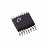
LTC2604IGN#TR Linear Technology, LTC2604IGN#TR Datasheet - Page 4

LTC2604IGN#TR
Manufacturer Part Number
LTC2604IGN#TR
Description
IC DAC 16BIT QUAD R-R OUT 16SSOP
Manufacturer
Linear Technology
Datasheet
1.LTC2624IGN-1PBF.pdf
(16 pages)
Specifications of LTC2604IGN#TR
Settling Time
10µs
Number Of Bits
16
Data Interface
Serial
Number Of Converters
4
Voltage Supply Source
Single Supply
Power Dissipation (max)
10mW
Operating Temperature
-40°C ~ 85°C
Mounting Type
Surface Mount
Package / Case
16-SSOP
Lead Free Status / RoHS Status
Contains lead / RoHS non-compliant
Available stocks
Company
Part Number
Manufacturer
Quantity
Price
LTC2604/LTC2614/LTC2624
ELECTRICAL CHARACTERISTICS
temperature range, otherwise specifi cations are at T
REF C = REF D = 2.048V (V
SYMBOL
V
V
V
I
C
The
A = REF B = REF C = REF D = 4.096V (V
unless otherwise noted. (Note 10)
SYMBOL PARAMETER
AC Performance
t
e
TIMING CHARACTERISTICS
range, otherwise specifi cations are at T
= 2.048V (V
SYMBOL
V
t
t
t
t
t
t
t
t
t
4
LK
1
2
3
4
5
6
7
8
9
s
IL
OH
OL
IN
n
CC
= 2.5V to 5.5V
●
denotes specifi cations which apply over the full operating temperature range, otherwise specifi cations are at T
Settling Time (Note 8)
Settling Time for
1LSB Step (Note 9)
Voltage Output Slew Rate
Capacitive Load Driving
Glitch Impulse
Multiplying Bandwidth
Output Voltage Noise
Density
Output Voltage Noise
CC
PARAMETER
Digital Input Low Voltage
Digital Output High Voltage
Digital Output Low Voltage
Digital Input Leakage
Digital Input Capacitance
PARAMETER
SDI Valid to SCK Setup
SDI Valid to SCK Hold
SCK High Time
SCK Low Time
CS/LD Pulse Width
LSB SCK High to CS/LD High
CS/LD Low to SCK High
SDO Propagation Delay from SCK Falling Edge
CLR Pulse Width
= 2.5V), REF LO = 0V, V
CC
= 2.5V), REF LO = 0V, V
CONDITIONS
±0.024% (±1LSB at 12 Bits)
±0.006% (±1LSB at 14 Bits)
±0.0015% (±1LSB at 16 Bits)
±0.024% (±1LSB at 12 Bits)
±0.006% (±1LSB at 14 Bits)
±0.0015% (±1LSB at 16 Bits)
At Midscale Transition
At f = 1kHz
At f = 10kHz
0.1Hz to 10Hz
OUT
CC
A
= 25°C. REF A = REF B = REF C = REF D = 4.096V (V
= 5V), REF A = REF B = REF C = REF D = 2.048V (V
unloaded, unless otherwise noted. (Note 10)
CONDITIONS
V
V
Load Current = –100μA
Load Current = +100μA
V
(Note 6)
CC
CC
IN
= GND to V
= 4.5V to 5.5V
= 2.5V to 5.5V
A
OUT
= 25°C. REF A = REF B = REF C = REF D = 4.096V (V
The
CONDITIONS
C
unloaded, unless otherwise noted. (Note 10)
LOAD
●
V
V
The
denotes specifi cations which apply over the full operating temperature
CC
CC
CC
= 10pF
= 4.5V to 5.5V
= 2.5V to 5.5V
●
denotes specifi cations which apply over the full operating
MIN
LTC2624/LTC2624-1
1000
0.80
TYP
180
120
100
2.7
12
15
7
MAX
LTC2614/LTC2614-1
MIN
CC
CC
1000
0.80
= 2.5V), REF LO = 0V, V
TYP
180
120
100
2.7
4.8
l
l
l
l
l
l
l
l
l
l
12
15
l
l
l
l
l
l
= 5V), REF A = REF B = REF C = REF D
7
9
V
CC
MAX
MIN
MIN
10
20
4
4
9
9
7
7
– 0.4
CC
LTC2604/LTC2604-1
MIN
= 5V), REF A = REF B =
TYP
TYP
1000
0.80
TYP
180
120
100
2.7
4.8
5.2
10
12
15
7
9
A
OUT
= 25°C. REF
MAX
MAX
0.8
0.6
0.4
±1
20
45
8
MAX
unloaded,
nV√Hz
nV√Hz
UNITS
UNITS
UNITS
nV • s
μV
2604fd
V/μs
kHz
P–P
μA
μs
μs
μs
μs
μs
μs
pF
ns
ns
ns
ns
ns
ns
ns
ns
ns
ns
pF
V
V
V
V


