LTC2704CGW-14#TRPBF Linear Technology, LTC2704CGW-14#TRPBF Datasheet - Page 8
LTC2704CGW-14#TRPBF
Manufacturer Part Number
LTC2704CGW-14#TRPBF
Description
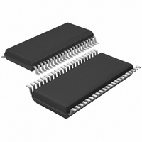
IC DAC 14BIT QUAD VOUT 44-SSOP
Manufacturer
Linear Technology
Datasheet
1.LTC2704IGW-12PBF.pdf
(22 pages)
Specifications of LTC2704CGW-14#TRPBF
Settling Time
9µs
Number Of Bits
14
Data Interface
Serial, SPI™
Number Of Converters
4
Voltage Supply Source
Analog and Digital, Dual ±
Operating Temperature
0°C ~ 70°C
Mounting Type
Surface Mount
Package / Case
44-SSOP
Lead Free Status / RoHS Status
Lead free / RoHS Compliant
Power Dissipation (max)
-
Available stocks
Company
Part Number
Manufacturer
Quantity
Price


TYPICAL PERFORMANCE CHARACTERISTICS
LTC2704
LTC2704-16/LTC2704-14/LTC2704-12
5V/DIV
PIN FUNCTIONS
V
Typically –15V. –4.5V to –16.5V Range.
REFG1 (Pin 2): Reference 1 Ground. High impedance
input, does not carry supply currents. Tie to clean analog
ground.
AGNDA (Pin 3): DAC A Signal Ground. High impedance
input, does not carry supply currents. Tie to clean analog
ground.
VOSA (Pin 4): Offset Adjust for DAC A. Nominal input
range is ±5V. V
±2.5V modes]. See Operation section.
8
–
(Pins 1, 8, 15, 22, 31, 36): Analog Negative Supply,
Positive Slew
V + /V
V
±10V RANGE
20V STEP
REF
–
= 5V
= ±15V
1μV/DIV
OS
2.5μs/DIV
(DAC A) = –0.01• V(VOSA) [0V to 5V,
0.1Hz to 10Hz Noise
V + /V
V
0V TO 5V RANGE
CODE = 0
REF
–
= 5V
= ±15V
1s/DIV
2704 G13
5V/DIV
2704 G16
Negative Slew
V + /V
V
±10V RANGE
20V STEP
REF
–
= 5V
= ±15V
2.5μs/DIV
C1A (Pin 5): Feedback Capacitor Connection for DAC A
Output. This pin provides direct access to the negative
input of the channel A output amplifi er.
OUTA (Pin 6): DAC A Voltage Output Pin. For best load
regulation, this open-loop amplifi er output is connected
to RFBA as close to the load as possible.
RFBA (Pin 7): DAC A Output Feedback Resistor Pin.
LDAC (Pin 9): Asynchronous DAC Load Input. When LDAC
is a logic low, all DACs are updated.
3.5
3.0
2.5
2.0
1.5
1.0
0.5
0
0
V
vs Logic Voltage
CC
0.5
Supply Current
2704 G14
1.0 1.5
LOGIC VOLTAGE (V)
2.0
2mV/DIV
2.5
V
SCK, SDI, CS/LD, LDAC
CLR TIED TOGETHER
5V/DIV
CS/LD
DD
V
OUT
3.0
= 5V
Midscale Glitch
3.5
4.0
4.5 5.0
2704 G17
2.5μs/DIV
2704fc
2704 G15
Related parts for LTC2704CGW-14#TRPBF
Image
Part Number
Description
Manufacturer
Datasheet
Request
R

Part Number:
Description:
IC,D/A CONVERTER,QUAD,16-BIT,CMOS,SOP,44PIN
Manufacturer:
Linear Technology
Datasheet:

Part Number:
Description:
IC DAC 12BIT QUAD VOUT 44-SSOP
Manufacturer:
Linear Technology
Datasheet:
Part Number:
Description:
IC DAC 12BIT QUAD VOUT 44-SSOP
Manufacturer:
Linear Technology
Datasheet:
Part Number:
Description:
IC DAC 16BIT QUAD VOUT 44-SSOP
Manufacturer:
Linear Technology
Datasheet:
Part Number:
Description:
IC DAC 14BIT QUAD VOUT 44-SSOP
Manufacturer:
Linear Technology
Datasheet:
Part Number:
Description:
IC DAC 16BIT QUAD VOUT 44-SSOP
Manufacturer:
Linear Technology
Datasheet:
Part Number:
Description:
IC,D/A CONVERTER,QUAD,12-BIT,CMOS,SOP,44PIN
Manufacturer:
Linear Technology
Part Number:
Description:
IC,D/A CONVERTER,QUAD,12-BIT,CMOS,SOP,44PIN
Manufacturer:
Linear Technology
Part Number:
Description:
IC,D/A CONVERTER,QUAD,14-BIT,CMOS,SOP,44PIN
Manufacturer:
Linear Technology
Part Number:
Description:
IC,D/A CONVERTER,QUAD,14-BIT,CMOS,SOP,44PIN
Manufacturer:
Linear Technology
Part Number:
Description:
IC,D/A CONVERTER,QUAD,16-BIT,CMOS,SOP,44PIN
Manufacturer:
Linear Technology

Part Number:
Description:
Quad 12-, 14- and 16-Bit Voltage Output SoftSpan DACs with Readback
Manufacturer:
LINER [Linear Technology]
Datasheet:
Part Number:
Description:
CD ROM LINEARVIEW DATASHEETS
Manufacturer:
Linear Technology

Part Number:
Description:
Standalone Linear Li-Ion Battery Charger with Thermal Regulation in ThinSOT
Manufacturer:
Linear Technology Corporation
Datasheet:
Part Number:
Description:
Low noise, high frequency, 8th order linear phase lowpass filter
Manufacturer:
Linear Technology Corporation
Datasheet: