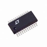
LTC1599AIG#PBF Linear Technology, LTC1599AIG#PBF Datasheet - Page 13

LTC1599AIG#PBF
Manufacturer Part Number
LTC1599AIG#PBF
Description
IC D/A CONV 16BIT MLTPLYNG24SSOP
Manufacturer
Linear Technology
Datasheet
1.LTC1599BCN.pdf
(20 pages)
Specifications of LTC1599AIG#PBF
Settling Time
1µs
Number Of Bits
16
Data Interface
Parallel
Number Of Converters
1
Voltage Supply Source
Single Supply
Power Dissipation (max)
55µW
Operating Temperature
-40°C ~ 85°C
Mounting Type
Surface Mount
Package / Case
24-SSOP
Number Of Channels
1
Resolution
16b
Interface Type
Parallel
Single Supply Voltage (typ)
5V
Dual Supply Voltage (typ)
Not RequiredV
Architecture
R-2R
Power Supply Requirement
Single
Output Type
Current
Integral Nonlinearity Error
±1LSB
Single Supply Voltage (min)
4.5V
Single Supply Voltage (max)
5.5V
Dual Supply Voltage (min)
Not RequiredV
Dual Supply Voltage (max)
Not RequiredV
Operating Temp Range
-40C to 85C
Operating Temperature Classification
Industrial
Mounting
Surface Mount
Pin Count
24
Package Type
SSOP
Lead Free Status / RoHS Status
Lead free / RoHS Compliant
or 10V full-scale systems. However, as the circuit band-
widths increase, filtering the output of the reference may
be required to minimize output noise.
Table 5. Partial List of LTC Precision References Recommended
for Use with the LTC1599, with Relevant Specifications
REFERENCE
LT1019A-5,
LT1019A-10
LT1236A-5,
LT1236A-10
LT1460A-5,
LT1460A-10
Grounding
As with any high resolution converter, clean grounding is
important. A low impedance analog ground plane and star
grounding should be used. I
to the star ground with as low a resistance as possible.
When it is not possible to locate star ground close to
I
these pins to star ground. This minimizes the voltage drop
from these pins to ground caused by the code dependent
current flowing to ground. When the resistance of these
circuit board traces becomes greater than 1Ω, the circuit
in Figure 4 eliminates voltage drop errors caused by high
APPLICATIONS
OUT2F
and I
15V
OUT2S
TOLERANCE
±0.075%
2
4
±0.05%
±0.05%
INITIAL
LT1236A-10
, separate traces should be used to route
MLBYTE
INPUTS
U
CLVL
14 TO 18,
DATA
21 TO 23
CLR
WR
LD
8
INFORMATION
13
TEMPERATURE
U
6 10V
OUT2F
MLBYTE
WR
4
R1
10ppm
DRIFT
5ppm
5ppm
12 11
Figure 4. Driving I
R1
LD
and I
CLR CLVL
LTC1599
W
3
R
24
COM
R2
OUT2S
10
2
R2
0.1Hz to 10Hz
must be tied
12µV
20µV
3µV
NOISE
OUT2F
1
REF
U
P-P
P-P
P-P
and I
DGND
5V
V
CC
19
20
OUT2S
R
5
R
OFS
0.1µF
OFS
resistance traces. This preserves the excellent accuracy
(1LSB INL and DNL) of the LTC1599.
A 16-Bit, 4mA to 20mA Current Loop Controller
for Industrial Applications
Modern process control systems must often deal with
legacy 4mA to 20mA analog current loops as a means of
interfacing with actuators and valves located at a distance.
The circuit in Figure 5 provides an output to a current loop
controlled by an LTC1599, a 16-bit current output DAC. A
dual rail-to-rail op amp (U1, LT1366) controls a P-channel
power FET (Q2) to produce a current mirror with a precise
8:1 ratio as defined by a resistor array. The input current
to this mirror circuit is produced by a grounded base
cascode stage using a high gain transistor (Q1). The use
of a bipolar transistor in this location results in an error
term associated with U1B and Q1’s base current (– 0.2%
for the device shown). For control applications however,
absolute accuracy of the output to an actuator is usually
not required. If a higher degree of absolute accuracy is
required, Q1 can be replaced with an N-channel JFET;
however, this requires a single amplifier at U1B with the
ability to drive the gate below ground. An enhancement
mode N-channel FET can be used in place of Q1 but
MOSFET leakage current must be considered and gate
overdrive must be avoided.
16-BIT DAC
with a Force/Sense Amplifier
R
FB
9
I
OUT2S
R
6
FB
I
OUT1
I
OUT2F
7
8
2
3
6
33pF
–
+
LT1001
LT1001
+
–
6
3
2
1599 F04
V
0V TO –10V
LTC1599
OUT
sn1599 1599fs
13


