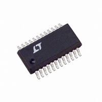
LTC1599AIG#PBF Linear Technology, LTC1599AIG#PBF Datasheet - Page 17

LTC1599AIG#PBF
Manufacturer Part Number
LTC1599AIG#PBF
Description
IC D/A CONV 16BIT MLTPLYNG24SSOP
Manufacturer
Linear Technology
Datasheet
1.LTC1599BCN.pdf
(20 pages)
Specifications of LTC1599AIG#PBF
Settling Time
1µs
Number Of Bits
16
Data Interface
Parallel
Number Of Converters
1
Voltage Supply Source
Single Supply
Power Dissipation (max)
55µW
Operating Temperature
-40°C ~ 85°C
Mounting Type
Surface Mount
Package / Case
24-SSOP
Number Of Channels
1
Resolution
16b
Interface Type
Parallel
Single Supply Voltage (typ)
5V
Dual Supply Voltage (typ)
Not RequiredV
Architecture
R-2R
Power Supply Requirement
Single
Output Type
Current
Integral Nonlinearity Error
±1LSB
Single Supply Voltage (min)
4.5V
Single Supply Voltage (max)
5.5V
Dual Supply Voltage (min)
Not RequiredV
Dual Supply Voltage (max)
Not RequiredV
Operating Temp Range
-40C to 85C
Operating Temperature Classification
Industrial
Mounting
Surface Mount
Pin Count
24
Package Type
SSOP
Lead Free Status / RoHS Status
Lead free / RoHS Compliant
APPLICATIONS
Interfacing to the 68HC11
The circuit in Figure 7 is an example of using the 68HC11
to control the LTC1599. Data is sent to the DAC using two
8-bit parallel transfers from the controller’s Port B. The
WR signal is generated by manipulating the logic output
on Port A’s bit 3, the MLBYTE command is sent to the DAC
using Port A’s bit 4, and the LD command comes from the
SS output on Port D’s bit 5.
The sample listing 68HC11 assembly code in Listing A is
designed to emulate the Timing Diagram found earlier in
this data sheet. After variable declaration, the main portion
of the program retrieves the least significant byte from
memory, forces MLBYTE and WR to a logic low, and then
writes the low byte data to Port B. It then sets WR and
************************************************************
*
* This example program uses 8-bit parallel port B, port A and port D
* to transfer 16-bit parallel data to the LTC1599 16-bit current output
* DAC. Port B at $1004 is used for two eight bit transfers. Port A,
* bit 3 is used for the LTC1599’s WR command and bit 4 is used for the
* MLBYTE command. Port D’ SS output is used for the LTC1599’s LD
* command
*
************************************************************
*
*****************************************
* 68HC11 register definitions
*****************************************
*
* PIOC
*
PORTA
*
PORTB
*
PORTD
*
DDRD
SPCR
MBYTE
LBYTE
*
*****************************************
* Start OUTDATA Routine
*****************************************
*
INIT1
*
*
* DDRD’s Bit5 is a 1 so that port D’s SS* pin is a general output
EQU
EQU
EQU
EQU
EQU
EQU
EQU
EQU
ORG
LDAA
STAA
LDAA
STAA
$1002
$1000
$1004
$1008
$1009
$1028
$00
$01
$C000
#$2F
PORTD
#$38
DDRD
U
Parallel I/O control register
“STAF,STAI,CWOM,HNDS, OIN, PLS, EGA,INVB”
Port A data register
“Bit7,Bit6,Bit5,Bit4,Bit3,Bit2,Bit1,Bit0”
Port B data register
“Bit7,Bit6,Bit5,Bit4,Bit3,Bit2,Bit1,Bit0”
Port D data register
“ - , - , SS* ,CSK ;MOSI,MISO,TxD ,RxD “
Port D data direction register
SPI control register
This memory location holds the LTC1599’s bits 15 - 08
This memory location holds the LTC1599’s bits 07 - 00
Program start location
-,-,1,0;1,1,1,1
-, -, SS*-Hi, SCK-Lo, MOSI-Hi, MISO-Hi, X, X
Keeps SS* a logic high when DDRD, Bit5 is set
-,-,1,1;1,0,0,0
SS* , SCK, MOSI are configured as Outputs
MISO, TxD, RxD are configured as Inputs
INFORMATION
U
W
*
*
U
*
*
*
*
*
*
*
*
MLBYTE high. Next, the most significant byte is copied
from memory and WR is again asserted low. The high byte
is written to Port B and WR is returned high. The transfer
of the 16 bits is completed by cycling the LD input low and
then high using the SS output on Port D.
Figure 7. Using the 68HC11 to Control the LTC1599
PORT A , BIT 4
PORT D, BIT 5
PORT A, BIT 3
68HC11
PORT B
8-BIT PARALLEL
WR LD MLBYTE
LTC1599
LTC1599
1599 F07
sn1599 1599fs
17


