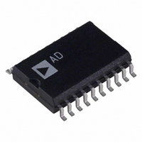
AD7302BR Analog Devices Inc, AD7302BR Datasheet - Page 5

AD7302BR
Manufacturer Part Number
AD7302BR
Description
IC DAC 8BIT DUAL 2.7V 20-SOIC
Manufacturer
Analog Devices Inc
Datasheet
1.AD7302BRUZ.pdf
(16 pages)
Specifications of AD7302BR
Mounting Type
Surface Mount
Rohs Status
RoHS non-compliant
Settling Time
1.2µs
Number Of Bits
8
Data Interface
Parallel
Number Of Converters
2
Voltage Supply Source
Single Supply
Power Dissipation (max)
24.8mW
Operating Temperature
-40°C ~ 105°C
Package / Case
20-SOIC (7.5mm Width)
Resolution (bits)
8bit
No. Of Pins
20
Update Rate
0.833MSPS
Peak Reflow Compatible (260 C)
No
Supply Voltage
5.5V
No. Of Bits
8 Bit
Leaded Process Compatible
No
Lead Free Status / RoHS Status
Contains lead / RoHS non-compliant
Available stocks
Company
Part Number
Manufacturer
Quantity
Price
Part Number:
AD7302BR
Manufacturer:
ADI/亚德诺
Quantity:
20 000
Company:
Part Number:
AD7302BRU
Manufacturer:
AD
Quantity:
4 130
Part Number:
AD7302BRUZ
Manufacturer:
ADI/亚德诺
Quantity:
20 000
Company:
Part Number:
AD7302BRZ
Manufacturer:
Maxim
Quantity:
25
Part Number:
AD7302BRZ
Manufacturer:
ADI/亚德诺
Quantity:
20 000
Part Number:
AD7302BRZ-REEL
Manufacturer:
ADI/亚德诺
Quantity:
20 000
REV. 0
Pin
No.
1-8
9
10
11
12
13
14
15
16
17
18
19
20
Mnemonic Function
D7–D0
CS
WR
A/B
PD
LDAC
CLR
V
REFIN
AGND
V
V
DGND
DD
OUT
OUT
B
A
Parallel Data Inputs. Eight-bit data is loaded to the input register of the AD7302 under the control of CS
and WR.
Chip Select. Active low logic input.
Write Input. WR is an active low logic input used in conjunction with CS and A/B to write data to the selected
DAC register.
DAC Select. Address pin used to select writing to either DAC A or DAC B.
Active low input used to put the part into low power mode reducing current consumption to less than 1 A.
Load DAC Logic Input. When this logic input is taken low both DAC outputs are simultaneously updated with
the contents of their DAC registers. If LDAC is permanently tied low, the DACs are updated on the rising
edge of WR.
Asynchronous Clear Input (Active Low). When this input is taken low the DAC registers are loaded with all
zeroes and the DAC outputs are cleared to zero volts.
Power Supply Input. These parts can be operated from 2.7 V to 5.5 V and should be decoupled to AGND.
External Reference Input. This can used as the reference for both DACs. The range on this reference input is
1 V to V
Analog Ground reference point and return point for all analog current on the part.
Analog output voltage from DAC B. The output amplifier can swing rail to rail on its output.
Analog output voltage from DAC A. The output amplifier can swing rail to rail on its output.
Digital Ground reference point and return point for all digital current on the part.
DD
/2. If REFIN is directly tied to V
PIN FUNCTION DESCRIPTIONS
(MSB) DB7
(LSB) DB0
PIN CONFIGURATION
DB6
DB5
DB4
DB3
DB2
DB1
WR
CS
10
1
2
3
4
5
6
7
8
9
(Not to Scale)
TOP VIEW
AD7302
DD
–5–
the internal V
20
19
18
17
16
15
14
13
12
11
DGND
V
V
AGND
REFIN
V
CLR
LDAC
PD
A/B
OUT
OUT
DD
A
B
DD
/2 reference is selected.
AD7302


