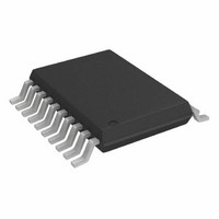
AD7801BRU Analog Devices Inc, AD7801BRU Datasheet

AD7801BRU
Specifications of AD7801BRU
Available stocks
Related parts for AD7801BRU
AD7801BRU Summary of contents
Page 1
FEATURES Single 8-Bit DAC 20-Pin SOIC/TSSOP Package +2 +5.5 V Operation Internal and External Reference Capability DAC Power-Down Function Parallel Interface On-Chip Output Buffer Rail-to-Rail Operation Low Power Operation 1.75 mA max @ 3.3 V Power-Down to ...
Page 2
AD7801–SPECIFICATIONS Parameter STATIC PERFORMANCE Resolution 2 Relative Accuracy Differential Nonlinearity Zero-Code Error @ +25 C Full-Scale Error Zero-Code Error Drift 3 Gain Error DAC REFERENCE INPUT REFIN Input Range REFIN Input Impedance OUTPUT CHARACTERISTICS Output Voltage Range Output Voltage Settling ...
Page 3
... Units ns min ns min ns min ns min ns min ns min ns min ns min Model + 0 0.3 V AD7801BR DD AD7801BRU + 0 Small Outline Thin Shrink Small Outline. –3– AD7801 /2 Reference. All specifications MIN MAX Conditions/Comments Chip Select to Write Setup Time Chip Select to Write Hold Time Write Pulse Width ...
Page 4
AD7801 Pin No. Mnemonic Function Parallel Data Inputs. 8-bit data is loaded to the input register of the AD7801 under the control of CS and WR. 1–8 D7– Chip Select. Active low logic input. WR Write Input. WR ...
Page 5
AND 3V 720 DD INTERNAL REFERENCE 640 DAC LOADED WITH 00HEX 560 480 400 320 240 160 SINK CURRENT – mA Figure 2. Output ...
Page 6
AD7801 –Typical Performance Characteristics OUT M20.0ms CH1 5.00V CH2 5.00V CH1 Figure 11. Power-On—Reset 0 0.4 INTERNAL REFERENCE 5k 100pF LOAD 0.3 LIMITED CODE RANGE (15–245 +25 ...
Page 7
TERMINOLOGY Integral Nonlinearity For the DAC, Relative Accuracy or End-Point nonlinearity is a measure of the maximum deviation, in LSBs, from a straight line passing through the endpoints of the DAC transfer function. A graphical representation of the transfer curve ...
Page 8
AD7801 Reference The AD7801 has the ability to use either an external reference applied through the REFIN pin or an internal reference generated from V . Figure 20 shows the reference input arrangement DD where either the internal V /2 ...
Page 9
POWER-ON RESET The AD7801 has a power-on reset circuit designed to allow output stability during power up. This circuit holds the DAC in a reset state until a write takes place to the DAC. In the reset state all zeros ...
Page 10
AD7801 Figure 27 shows a typical setup for the AD7801 when using its internal reference. The internal reference is selected by tying the REFIN pin Internally in the reference section there reference detect circuit ...
Page 11
In the circuit shown the LDAC is hardwired low thus the DAC output is updated on the rising edge of WR. Some applications may require synchronous updating of the DAC in the AD7801. In this case the LDAC signal can ...
Page 12
AD7801 AD7801 as a Digitally Programmable Indicator A digitally programmable upper limit detector using the DAC is shown in Figure 34. The upper limit for the test is loaded to the DAC, which in turn sets the limit for the ...
Page 13
Power Supply Bypassing and Grounding In any circuit where accuracy is important, careful consideration of the power supply and ground return layout helps to ensure the rated performance. The printed circuit board on which the AD7801 is mounted should be ...
Page 14
AD7801 0.0118 (0.30) 0.0040 (0.10) 0.006 (0.15) 0.002 (0.05) SEATING OUTLINE DIMENSIONS Dimensions shown in inches and (mm). 20-Lead Wide Body SOIC (R-20) 0.5118 (13.00) 0.4961 (12.60 PIN 1 0.1043 (2.65) 0.0926 (2.35) 0.0500 0.0192 (0.49) ...
Page 15
–15– ...
Page 16
–16– ...


