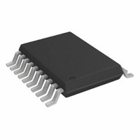
AD7801BRU Analog Devices Inc, AD7801BRU Datasheet - Page 10

AD7801BRU
Manufacturer Part Number
AD7801BRU
Description
IC DAC 8BIT PARALLEL INP 20TSSOP
Manufacturer
Analog Devices Inc
Datasheet
1.AD7801BRUZ-REEL.pdf
(16 pages)
Specifications of AD7801BRU
Rohs Status
RoHS non-compliant
Settling Time
1.2µs
Number Of Bits
8
Data Interface
Parallel
Number Of Converters
1
Voltage Supply Source
Single Supply
Power Dissipation (max)
12.9mW
Operating Temperature
-40°C ~ 105°C
Mounting Type
Surface Mount
Package / Case
20-TSSOP
Available stocks
Company
Part Number
Manufacturer
Quantity
Price
Part Number:
AD7801BRU
Manufacturer:
AD
Quantity:
20 000
Part Number:
AD7801BRUZ
Manufacturer:
ADI/亚德诺
Quantity:
20 000
Part Number:
AD7801BRUZ#
Manufacturer:
ADI/亚德诺
Quantity:
20 000
Part Number:
AD7801BRUZ-REEL
Manufacturer:
ADI/亚德诺
Quantity:
20 000
Part Number:
AD7801BRUZ-REEL7
Manufacturer:
ADI/亚德诺
Quantity:
20 000
AD7801
Figure 27 shows a typical setup for the AD7801 when using its
internal reference. The internal reference is selected by tying the
REFIN pin to V
reference detect circuit that will select the internal V
on the voltage connected to the REFIN pin. If REFIN is within
a threshold voltage of a PMOS device (approximately 1 V) of
V
is more than 1 V below V
this pin is used as the reference for the DAC. The internal
reference on the AD7801 is V
voltage converter within the AD7801 provides a gain of two.
Thus the output range of the DAC is from 0 V to V
Table I.
Figure 28 shows a typical setup for the AD7801 when using an
external reference. The reference range for the AD7801 is from
1 V to V
but will saturate the output at both the top and bottom end of
the transfer function. There is a gain of two from input to output
on the AD7801. Suitable references for 5 V operation are the
AD780 and REF192. For 3 V operation a suitable external
reference would be the AD589 a 1.23 V bandgap reference.
Figure 27. Typical Configuration Selecting the Internal
Reference
DD
AD780/REF192 WITH V
Figure 28. Typical Configuration Using An External
Reference
the internal reference is selected. When the REFIN voltage
AD589 WITH V
EXT REF
DD
/2 V. Higher values of reference can be incorporated
GND
V
OR
IN
0.1 F
V
DD
DD
DD
V
OUT
= 3V
DD
. Internally in the reference section there is a
= 5V
DATA BUS
REF IN
CLR
PD
10 F
D7-D0
0.1 F
0.1 F
DD
V
V
DD
DD
, the externally applied voltage at
AD7801
V
= 3V TO 5V
DD
DD
CONTROL
CS WR
10 F
INPUTS
DATA BUS
REF IN
CLR
PD
/2, the output current to
AGND DGND
D7-D0
V
DD
LDAC
AD7801
V
V
= 3V TO 5V
DD
OUT
CONTROL
CS WR LDAC
INPUTS
AGND DGND
V
OUT
DD
V
DD
OUT
, based on
/2 based
V
OUT
–10–
MICROPROCESSOR INTERFACING
AD7801–ADSP-2101/ADSP-2103 Interface
Figure 29 shows an interface between the AD7801 and the ADSP-
2101/ADSP-2103. The fast interface timing associated with the
AD7801 allows easy interface to the ADSP-2101/ADSP-2103.
LDAC is permanently tied low in this circuit so the DAC
output is updated on the rising edge of the WR signal.
Data is loaded to the AD7801 input register using the following
ADSP-21xx instruction.
MR0 = ADSP-21xx MR0 Register.
DAC = Decoded DAC Address.
AD7801–TMS320C20 Interface
Figure 30 shows an interface between the AD7801 and the
TMS320C20. Data is loaded to the AD7801 using the following
instruction:
DAC = Decoded DAC Address.
D = Data Memory Address.
TMS320C20
ADSP-2101*/
ADSP-2103*
Figure 29. AD7801–ADSP-2101/ADSP-2103 Interface
Figure 30. AD7801–TMS320C20 Interface
DMA14
DMD15
STRB
DMA0
DMD0
R/W
A15
D15
DMS
A0
D0
WR
IS
*
ADDITIONAL CIRCUITRY OMITTED FOR CLARITY.
*
ADDITIONAL CIRCUITRY OMITTED FOR CLARITY.
EN
DM(DAC) = MR0
EN
OUT DAC, D
DECODE
DECODE
ADDR
ADDR
ADDRESS BUS
ADDRESS BUS
DATA BUS
DATA BUS
CS
LDAC
WR
DB7
DB0
CS
LDAC
WR
DB7
DB0
AD7801*
AD7801*
REV. 0


