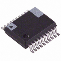
AD7948ARS-BREEL Analog Devices Inc, AD7948ARS-BREEL Datasheet - Page 13

AD7948ARS-BREEL
Manufacturer Part Number
AD7948ARS-BREEL
Description
IC DAC 12BIT MULT PARALL 20-SSOP
Manufacturer
Analog Devices Inc
Datasheet
1.AD7943BNZ.pdf
(16 pages)
Specifications of AD7948ARS-BREEL
Rohs Status
RoHS non-compliant
Settling Time
600ns
Number Of Bits
12
Data Interface
Parallel
Number Of Converters
1
Voltage Supply Source
Single Supply
Power Dissipation (max)
25µW
Operating Temperature
-40°C ~ 85°C
Mounting Type
Surface Mount
Package / Case
20-SSOP
REV. B
GENERAL DESCRIPTION
D/A Section
The AD7943, AD7945 and AD7948 are 12-bit current-output
D/A converters. A simplified circuit diagram is shown in Fig-
ure 13. The DAC architecture is segmented. This means that
the 2 MSBs of the 12-bit data word are decoded to drive the
three switches A, B and C. The remaining 10 bits of the data
word drive the switches S0 to S9 in a standard inverting R-2R
ladder configuration.
Each of the switches A to C steers 1/4 of the total reference
current into either I
total current passing through the R-2R section. Switches S9 to
S0 steer binarily weighted currents into either I
I
rent flows in each ladder leg, regardless of digital input code.
Thus, the input resistance seen at V
equal to R/2. The V
voltage or current, ac or dc that is within the Absolute Maxi-
mum Ratings.
The device provides access to the V
nals of the DAC. This makes the device extremely versatile and
allows it to be configured in several different operating modes.
Examples of these are shown in the following sections. The
AD7943 also has a separate I
AD7948 this is internally tied to AGND.
When an output amplifier is connected in the standard configu-
ration of Figure 14, the output voltage is given by:
where D is the fractional representation of the digital word
loaded to the DAC. D can be set from 0 to 4095/4096, since it
has 12-bit resolution.
OUT1
C
V
2R
and I
REF
B
Figure 13. Simplified D/A Circuit Diagram
OUT2
2R
A
are kept at the same potential, a constant cur-
2R
OUT1
R
REF
S9
SHOWN FOR ALL 1
V
input may be driven by any reference
OUT
or I
2R
R
OUT2
= –D
OUT2
S8
2R
with the remaining 1/4 of the
pin. In the AD7945 and
REF
REF
S
V
ON DAC
REF
, R
R
is always constant. It is
S0
FB
, and I
2R
OUT1
2R
OUT1
or I
R/2
OUT2
termi-
R
I
I
OUT2
OUT1
FB
. If
–13–
UNIPOLAR BINARY OPERATION
(Two-Quadrant Multiplication)
Figure 14 shows the standard unipolar binary connection dia-
gram for the AD7943, AD7945 and AD7948. When V
ac signal, the circuit performs two-quadrant multiplication.
Resistors R1 and R2 allow the user to adjust the DAC gain
error. With a specified gain error of 2 LSBs over temperature,
these are not necessary in many applications. Circuit offset is
due completely to the output amplifier offset. It can be re-
moved by adjusting the amplifier offset voltage. Alternatively,
choosing a low offset amplifier makes this unnecessary.
A1 should be chosen to suit the application. For example, the
OP07 is ideal for very low bandwidth applications (10 kHz or
lower) while the AD711 is suitable for medium bandwidth ap-
plications (200 kHz or lower). For high bandwidth applications
of greater than 200 kHz, the AD843 and AD847 offer very fast
settling times.
The code table for Figure 14 is shown in Table III.
Digital Input
MSB
1111 1111 1111
1000 0000 0001
1000 0000 0000
0111 1111 1111
0000 0000 0001
0000 0000 0000
NOTE
Nominal LSB size for the circuit of Figure 14 is given by: V
V
IN
NOTES
1. ONLY ONE DAC IS SHOWN FOR CLAIRITY.
2. DIGITAL INPUT CONNECTIONS ARE OMITTED.
3. C1 PHASE COMPENSATION (5 – 15pF) MAY BE REQUIRED
WHEN USING HIGH SPEED AMPLIFIER.
LSB
R1 20
Figure 14. Unipolar Binary Operation
V
Table III. Unipolar Binary Code
REF
AD7943/AD7945/AD7948
AD7943/45/48
DAC
RFB
Analog Output
(V
–V
–V
–V
–V
–V
–V
OUT
REF
REF
REF
REF
REF
REF
(0/4096) = 0
(4095/4096)
(2049/4096)
(2048/4096)
(2047/4096)
(1/4096)
as Shown in Figure 14)
R2 10
AGND
I
I
OUT1
OUT2
SIGNAL GROUND
C1
A1
REF
A1: OP07
(1/4096).
AD711
AD843
AD845
IN
V
OUT
is an


