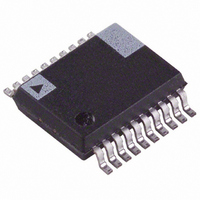
AD7948ARS-BREEL Analog Devices Inc, AD7948ARS-BREEL Datasheet - Page 15

AD7948ARS-BREEL
Manufacturer Part Number
AD7948ARS-BREEL
Description
IC DAC 12BIT MULT PARALL 20-SSOP
Manufacturer
Analog Devices Inc
Datasheet
1.AD7943BNZ.pdf
(16 pages)
Specifications of AD7948ARS-BREEL
Rohs Status
RoHS non-compliant
Settling Time
600ns
Number Of Bits
12
Data Interface
Parallel
Number Of Converters
1
Voltage Supply Source
Single Supply
Power Dissipation (max)
25µW
Operating Temperature
-40°C ~ 85°C
Mounting Type
Surface Mount
Package / Case
20-SSOP
REV. B
MICROPROCESSOR INTERFACING
AD7943 to ADSP-2101 Interface
Figure 17 shows the AD7943 to ADSP-2101 interface diagram.
The DSP is set up for alternate inverted framing with an inter-
nally generated SCLK. TFS from the ADSP-2101 drives the
STB1 input on the AD7943. The serial word length should be
set at 12. This is done by making SLEN = 11 (1011 binary).
The SLEN field is Bits 3–0 in the SPORT control register
(0x3FF6 for SPORT0 and 0x3FF2 for SPORT1).
With the 16 MHz version of the ADSP-2101, the maximum
output SCLK is 8 MHz. The AD7943 setup and hold time of
10 ns and 25 ns mean that it is compatible with the DSP when
running at this speed.
The OUTPUT FLAG drives both LD1 and LD2 and is brought
low to update the DAC register and change the analog output.
AD7943 to DSP56001 Interface
Figure 18 shows the interface diagram for the AD7943 to the
DSP56001. The DSP56001 is configured for normal mode
synchronous operation with gated clock. The serial clock, SCK,
is set up as an output from the DSP and the serial word length
is set for 12 bits (WL0 = 1, WL1 = 0, in Control Register A).
SCK from the DSP56001 is applied to the AD7943 STB3 in-
put. Data from the DSP56000 is valid on the falling edge of
SCK and this is the edge which clocks the data into the AD7943
shift register. STB1, STB2 and STB4 are tied low on the
AD7943 to permanently enable the STB3 input.
When the 12-bit serial word has been written to the AD7943,
the LD1, LD2 inputs are brought low to update the DAC
register.
ADSP-2101
DSP56001
OUTPUT FLAG
OUTPUT FLAG
Figure 17. AD7943 to ADSP-2101 Interface
Figure 18. AD7943 to DSP56001 Interface
SCLK
TFS
SCK
STD
DT
+5V
+5V
CLR
STB3
SRI
LD1
LD2
STB1
CLR
STB1
STB3
SRI
LD1
LD2
STB2
AD7943
STB2
AD7943
STB4
STB4
–15–
AD7945 to MC68000 Interface
Figure 19 shows the MC68000 interface to the AD7945. The
appropriate data is written into the DAC in one MOVE instruc-
tion to the appropriate memory location.
AD7948 to Z80 Interface
Figure 20 is the interface between the AD7948 and the 8-bit
bus of the Z80 processor. Three write operations are needed to
load the DAC. The first two load the MS byte and the LS byte
and the third brings the LDAC low to update the output.
MC68000
Z80
A1 – A23
D15 – D0
A0 – A15
Figure 19. AD7945 to MC68000 Interface
D7 – D0
DTACK
MREQ
R/W
Figure 20. AD7948 to Z80 Interface
WR
AS
AD7943/AD7945/AD7948
ADDRESS
ADDRESS
DECODE
DECODE
DATA BUS
ADDRESS BUS
CS
WR
DB11 – DB0
CSLSB
LDAC
DB7 – DB0
CSMSB
WR
AD7945
AD7948


