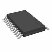
AD5334BRUZ Analog Devices Inc, AD5334BRUZ Datasheet - Page 3

AD5334BRUZ
Manufacturer Part Number
AD5334BRUZ
Description
IC DAC 8BIT QUAD VOUT 24-TSSOP
Manufacturer
Analog Devices Inc
Datasheet
1.AD5336BRUZ.pdf
(20 pages)
Specifications of AD5334BRUZ
Data Interface
Parallel
Settling Time
6µs
Number Of Bits
8
Number Of Converters
4
Voltage Supply Source
Single Supply
Power Dissipation (max)
4.5mW
Operating Temperature
-40°C ~ 105°C
Mounting Type
Surface Mount
Package / Case
24-TSSOP
Resolution (bits)
8bit
Sampling Rate
167kSPS
Input Channel Type
Parallel
Supply Voltage Range - Analog
2.5V To 5.5V
Supply Current
600µA
Number Of Channels
4
Resolution
8b
Conversion Rate
167KSPS
Interface Type
Parallel
Single Supply Voltage (typ)
3.3/5V
Dual Supply Voltage (typ)
Not RequiredV
Architecture
Resistor-String
Power Supply Requirement
Single
Output Type
Voltage
Integral Nonlinearity Error
±1LSB
Single Supply Voltage (min)
2.5V
Single Supply Voltage (max)
5.5V
Dual Supply Voltage (min)
Not RequiredV
Dual Supply Voltage (max)
Not RequiredV
Operating Temp Range
-40C to 105C
Operating Temperature Classification
Industrial
Mounting
Surface Mount
Pin Count
24
Package Type
TSSOP
Lead Free Status / RoHS Status
Lead free / RoHS Compliant
Lead Free Status / RoHS Status
Lead free / RoHS Compliant, Lead free / RoHS Compliant
Available stocks
Company
Part Number
Manufacturer
Quantity
Price
Part Number:
AD5334BRUZ
Manufacturer:
ADI/亚德诺
Quantity:
20 000
AC CHARACTERISTICS
Parameter
Output Voltage Settling Time
Slew Rate
Major Code Transition Glitch Energy
Digital Feedthrough
Digital Crosstalk
Analog Crosstalk
DAC-to-DAC Crosstalk
Multiplying Bandwidth
Total Harmonic Distortion
NOTES
1
2
3
Specifications subject to change without notice.
TIMING CHARACTERISTICS
Parameter
t
t
t
t
t
t
t
t
t
t
t
t
t
t
t
NOTES
1
2
3
Specifications subject to change without notice.
REV. 0
Guaranteed by design and characterization, not production tested.
See Terminology section.
Temperature range: B Version: –40°C to +105°C; typical specifications are at 25°C.
Guaranteed by design and characterization, not production tested.
All input signals are specified with tr = tf = 5 ns (10% to 90% of V
See Figure 1.
1
2
3
4
5
6
7
8
9
10
11
12
13
14
15
and timed from a voltage level of (V
AD5334
AD5335
AD5336
AD5344
2
Limit at T
0
0
20
5
4.5
5
5
4.5
5
4.5
20
20
50
20
0
IL
+ V
1
IH
(V
wise noted.)
MIN
)/2.
DD
, T
= 2.5 V to 5.5 V. R
1, 2, 3
MAX
Min
(V
B Version
DD
= 2.5 V to 5.5 V, All specifications T
Typ
6
7
7
8
0.7
8
0.5
3
0.5
3.5
200
–70
DD
Unit
ns min
ns min
ns min
ns min
ns min
ns min
ns min
ns min
ns min
ns min
ns min
ns min
ns min
ns min
ns min
)
L
= 2 k
3
Max
8
9
9
10
–3–
to GND; C
LDAC
LDAC
DATA,
HBEN
GAIN,
CLR
Unit
µs
µs
µs
µs
V/µs
nV-s
nV-s
nV-s
nV-s
nV-s
kHz
dB
WR
A0,
L
CS
A1
= 200 pF to GND. All specifications T
2
1
Figure 1. Parallel Interface Timing Diagram
Condition/Comments
CS to WR Setup Time
CS to WR Hold Time
WR Pulsewidth
Data, GAIN, HBEN Setup Time
Data, GAIN, HBEN Hold Time
Synchronous Mode. WR Falling to LDAC Falling.
Synchronous Mode. LDAC Falling to WR Rising.
Synchronous Mode. WR Rising to LDAC Rising.
Asynchronous Mode. LDAC Rising to WR Rising.
Asynchronous Mode. WR Rising to LDAC Falling.
LDAC Pulsewidth
CLR Pulsewidth
Time Between WR Cycles
A0, A1 Setup Time
A0, A1 Hold Time
NOTES:
1
2
SYNCHRONOUS LDAC UPDATE MODE
ASYNCHRONOUS LDAC UPDATE MODE
AD5334/AD5335/AD5336/AD5344
Conditions/Comments
V
1/4 Scale to 3/4 Scale Change (40 H to C0 H)
1/4 Scale to 3/4 Scale Change (100 H to 300 H)
1/4 Scale to 3/4 Scale Change (100 H to 300 H)
1/4 Scale to 3/4 Scale Change (400 H to C00 H)
1 LSB Change Around Major Carry
V
V
MIN
REF
REF
REF
t
1
to T
= 2 V. See Figure 20
= 2 V ± 0.1 V p-p. Unbuffered Mode
= 2.5 V ± 0.1 V p-p. Frequency = 10 kHz
MAX
t
6
unless otherwise noted.)
t
3
t
t
t
t
14
7
9
4
t
t
t
t
2
8
5
15
t
10
MIN
t
13
to T
MAX
t
11
unless other-
t
12


