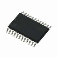
CS43L42-KZZ Cirrus Logic Inc, CS43L42-KZZ Datasheet - Page 24

CS43L42-KZZ
Manufacturer Part Number
CS43L42-KZZ
Description
IC DAC W/HDPN AMP LV 24TSSOP
Manufacturer
Cirrus Logic Inc
Datasheet
1.CS43L42-KZZ.pdf
(40 pages)
Specifications of CS43L42-KZZ
Number Of Bits
24
Data Interface
Serial
Number Of Converters
2
Voltage Supply Source
Single Supply
Power Dissipation (max)
41mW
Operating Temperature
-10°C ~ 70°C
Mounting Type
Surface Mount
Package / Case
24-TSSOP
Lead Free Status / RoHS Status
Lead free / RoHS Compliant
Settling Time
-
Other names
598-1651
Available stocks
Company
Part Number
Manufacturer
Quantity
Price
Company:
Part Number:
CS43L42-KZZ
Manufacturer:
CIRRUS
Quantity:
148
Part Number:
CS43L42-KZZ
Manufacturer:
CIRRUSLOGIC
Quantity:
20 000
4.11 Mode Control 2 (address 0Bh)
4.11.1 MASTER CLOCK DIVIDE ENABLE (MCLKDIV)
4.11.2 LINE AMPLIFIER GAIN COMPENSATION (LINE)
4.11.3 DIGITAL INTERFACE FORMAT (DIF)
24
MCLKDIV
Function:
Function:
Function:
7
0
Note:
Note:
Default = 0
0 - Disabled
1 - Enabled
The MCLKDIV bit enables a circuit which divides the externally applied MCLK signal by 2 prior to all other
internal circuitry.
Note:
Default = 00
00 - 0.785 x VA
01 - 0.943 x VA
10 - 1.571 x VA
11 - Line Mute
The Line Amplifier Gain Compensation bits allow the user to scale the full-scale line output level according
to the power supply voltage used. The full-scale line output level will be equal to {gain factor}xVA, where
{gain factor} is selected from options above. For example, if the user wants the full-scale line output volt-
age to be 1 V
1.571.
The Line Mute option is available to allow muting of the line output when the headphone output is still in
use and the line amp is still powered up. To use this feature, first mute the outputs via the ATAPI bits.
Next, set the LINE GAIN to Line Mute. Finally, un-mute the outputs with the ATAPI bits. Following these
steps will ensure a click free mute.
Default = 000 - Format 0 (I
The required relationship between the Left/Right clock, serial clock and serial data is defined by the Digital
Interface Format and the options are detailed in Figures 19-25.
LINE1
Internal SCLK is not available when this function is enabled.
It is possible to exceed the maximum output level, limited by VA_LINE, by incorrectly setting the
gain compensation factor.
Internal SCLK is not available when MCLKDIV is enabled.
6
0
RMS
(2.8 V
LINE0
PP
5
0
) with VA = 1.8 VDC and VA_LINE = 3.0 VDC, then the gain factor would be
2
S, up to 24-bit data, 64 x Fs Internal SLCK)
RESERVED
4
0
RESERVED
3
0
DIF2
2
0
DIF1
1
0
CS43L42
DS481PP2
DIF0
0
0


