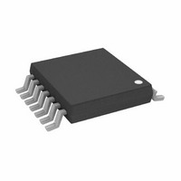
AD5666BRUZ-1 Analog Devices Inc, AD5666BRUZ-1 Datasheet

AD5666BRUZ-1
Specifications of AD5666BRUZ-1
Available stocks
Related parts for AD5666BRUZ-1
AD5666BRUZ-1 Summary of contents
Page 1
FEATURES Low power quad 16-bit DAC 14-lead TSSOP On-chip 1.25 V/2 ppm/°C reference Power down to 400 200 2 5.5 V power supply Guaranteed monotonic by design Power-on ...
Page 2
AD5666 TABLE OF CONTENTS Features .............................................................................................. 1 Applications ....................................................................................... 1 Functional Block Diagram .............................................................. 1 General Description ......................................................................... 1 Product Highlights ........................................................................... 1 Revision History ............................................................................... 2 Specifications ..................................................................................... 3 AC Characteristics ........................................................................ 7 Timing Characteristics ................................................................ 8 Absolute Maximum ...
Page 3
SPECIFICATIONS kΩ to GND Table 1. Parameter Min 2 STATIC PERFORMANCE Resolution 16 Relative Accuracy Differential Nonlinearity Zero-Code Error Zero-Code Error Drift Full-Scale Error Gain Error Gain ...
Page 4
AD5666 Parameter Min 3 LOGIC OUTPUTS (SDO) Output Low Voltage Output High Voltage − High Impedance Leakage Current High Impedance Output Capacitance POWER REQUIREMENTS V 4 (Normal Mode ...
Page 5
kΩ to GND Table 2. A Grade Parameter Min STATIC PERFORMANCE 2 Resolution 16 Relative Accuracy Differential Nonlinearity Zero-Code Error Zero-Code Error Drift Full-Scale Error Gain Error ...
Page 6
AD5666 A Grade Parameter Min Current POWER REQUIREMENTS V 2 (Normal Mode (All Power-Down Modes ...
Page 7
AC CHARACTERISTICS V =2. kΩ to GND Table Parameter Min Output Voltage Settling Time Slew Rate Digital-to-Analog Glitch Impulse Reference Feedthrough SDO Feedthrough Digital Feedthrough Digital Crosstalk Analog ...
Page 8
AD5666 TIMING CHARACTERISTICS All input signals are specified with ns/V (10 Figure 2 5.5 V. All specifications T DD Table 4. Limit ...
Page 9
SCLK SYNC DIN DB31 1 LDAC 2 LDAC CLR 1 ASYNCHRONOUS LDAC UPDATE MODE 2 SYNCHRONOUS LDAC UPDATE MODE SCLK SYNC ...
Page 10
AD5666 ABSOLUTE MAXIMUM RATINGS T = 25°C, unless otherwise noted. A Table 5. Parameter Rating V to GND −0 Digital Input Voltage to GND −0 GND −0 ...
Page 11
PIN CONFIGURATION AND FUNCTION DESCRIPTIONS Table 6. Pin Function Descriptions Pin No. Mnemonic Description 1 LDAC Pulsing this pin low allows any or all DAC registers to be updated if the input registers have new data. This allows all DAC ...
Page 12
AD5666 TYPICAL PERFORMANCE CHARACTERISTICS REF 25° –2 –4 –6 –8 – 10k 15k 20k 25k 30k 35k 40k 45k 50k 55k 60k 65k ...
Page 13
–0.02 –0.04 GAIN ERROR –0.06 –0.08 –0.10 –0.12 –0.14 FULL-SCALE ERROR –0.16 –0.18 –0.20 –40 – TEMPERATURE (°C) Figure 12. Gain Error and Full-Scale Error vs. Temperature 1.5 1.0 ZERO-SCALE ERROR ...
Page 14
AD5666 0.50 DAC LOADED WITH DAC LOADED WITH 0.40 FULL-SCALE ZERO-SCALE SOURCING CURRENT SINKING CURRENT 0. 1.25V REFOUT 0 –0.10 –0. –0. 2.5V REFOUT –0.40 –0.50 ...
Page 15
T = 25°C A 3.5 3.0 2.5 2 1.5 DD 1.0 0 (V) LOGIC Figure 24. Supply Current vs. Logic Input Voltage ...
Page 16
AD5666 2.5000 2.4995 2.4990 2.4985 2.4980 2.4975 2.4970 2.4965 2.4960 2.4955 2.4950 0 64 128 192 256 SAMPLE Figure 30. Analog Crosstalk 2.4900 2.4895 2.4890 2.4885 2.4880 2.4875 2.4870 2.4865 2.4860 2.4855 0 64 128 192 256 SAMPLE Figure 31. ...
Page 17
25°C A –30 DAC LOADED WITH FULL SCALE = 2V ± 0.3Vp-p V REF –40 –50 –60 –70 –80 –90 –100 FREQUENCY (Hz) Figure 36. Total Harmonic Distortion 16 V ...
Page 18
AD5666 TERMINOLOGY Relative Accuracy For the DAC, relative accuracy, or integral nonlinearity (INL measure of the maximum deviation in LSBs from a straight line passing through the endpoints of the DAC transfer function. Figure 6 shows a plot ...
Page 19
Digital Crosstalk Digital crosstalk is the glitch impulse transferred to the output of one DAC at midscale in response to a full-scale code change (all 0s to all 1s or vice versa) in the input register of another DAC. It ...
Page 20
AD5666 THEORY OF OPERATION D/A SECTION The AD5666 DAC is fabricated on a CMOS process. The archi- tecture consists of a string of DACs followed by an output buffer amplifier. The parts include an internal 1.25 V/2 ppm/°C ...
Page 21
OUTPUT AMPLIFIER The output buffer amplifier can generate rail-to-rail voltages on its output, which gives an output range amplifier is capable of driving a load of 2 kΩ in parallel with 1000 pF to GND. ...
Page 22
AD5666 INPUT SHIFT REGISTER The input shift register is 32 bits wide (see Figure 42). The first four bits are don’t cares. The next four bits are the command bits (see Table 8), followed by the 4-bit ...
Page 23
DAISY-CHAINING For systems that contain several DACs, or where the user wishes to read back the DAC contents for diagnostic purposes, the SDO pin can be used to daisy-chain several devices together and provide serial readback. The daisy-chain mode is ...
Page 24
AD5666 Table 9. Daisy-Chain Enable/Internal Reference Register DCEN (DB1 Table 10. 32-Bit Input Shift Register Contents for Daisy-Chain Enable and Reference Set-Up Function MSB DB31 to DB28 DB27 DB26 DB25 Don’t cares ...
Page 25
CLEAR CODE REGISTER The AD5666 has a hardware CLR pin that is an asynchronous clear input. The CLR input is falling edge sensitive. Bringing the CLR line low clears the contents of the input register and the DAC registers to ...
Page 26
AD5666 Table 13. Clear Code Register Clear Code Register DB1 DB0 CR1 CR0 Clears to Code 0 0 0x0000 0 1 0x8000 1 0 0xFFFF operation Table 14. 32-Bit Input Shift Register Contents for Clear Code Function ...
Page 27
... COPLANARITY 0.10 ORDERING GUIDE 1 Model Temperature Range AD5666BRUZ-1 −40°C to +105°C AD5666BRUZ-1REEL7 −40°C to +105°C AD5666BRUZ-2 −40°C to +105°C AD5666BRUZ-2REEL7 −40°C to +105°C AD5666ARUZ-2 −40°C to +105°C AD5666ARUZ-2REEL7 −40°C to +105°C EVAL-AD5666EBZ RoHS Compliant Part ...
Page 28
AD5666 NOTES ©2005–2010 Analog Devices, Inc. All rights reserved. Trademarks and registered trademarks are the property of their respective owners. D05298–0–6/10(D) Rev Page ...


