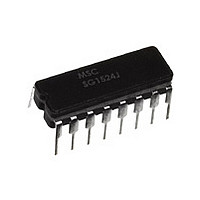
7802801EA MICROSEMI, 7802801EA Datasheet - Page 4

7802801EA
Manufacturer Part Number
7802801EA
Description
Manufacturer
MICROSEMI
Datasheet
1.7802801EA.pdf
(6 pages)
Specifications of 7802801EA
Number Of Pwm Outputs
2
On/off Pin
Yes
Adjustable Output
No
Topology
Push-Pull
Switching Freq
300KHz
Operating Supply Voltage (max)
40V
Synchronous Pin
No
Operating Temperature Classification
Military
Mounting
Through Hole
Pin Count
16
Package Type
CDIP
Lead Free Status / Rohs Status
Supplier Unconfirmed
Available stocks
Company
Part Number
Manufacturer
Quantity
Price
Rev 1.1a
Copyright
APPLICATION NOTES
OSCILLATOR
establish a constant charging current into an external capacitor
C
provides a linear ramp voltage at C
dependent reference for the PWM comparator. The charging
current is equal to 3.6V/R
30 A and 2mA. The equivalent range for R
The range of values for C
of C
The pulse is used (among other things) as a blanking pulse to
both outputs to insure that there is no possibility of having both
outputs on simultaneously during transitions.
deadtime relationship is shown in Figure 1. A pulse width below
0.35 microseconds may cause failure of the internal flip-flop to
toggle. This restricts the minimum value of C
Although the oscillator output is a convenient oscilloscope sync
input, the probe capacitance will increase the pulse width and
decrease the oscillator frequency slightly.) Obviously, the upper
limit to the pulse width is determined by the modulation range
required in the power supply at the chosen switching frequency.
Practical values of C
successful 120 Hz oscillators have been implemented with val-
ues up to 5 F and a series surge limit resistor of 100 ohms.
The oscillator frequency is approximately 1/R
ohms, C is in microfarads, and the frequency is in Megahertz. For
greater accuracy, the chart in Figure 2 may be used for a wide
range of operating frequencies.
The oscillator in the SG1524 uses an external resistor R
T
. While this uses more current than a series-connected RC, it
T
determines the pulse width of the oscillator output pulse.
1994
FIGURE 1 - OUTPUT STAGE DEADTIME VS. C
T
fall between 1000pF and 0.1 F, although
T
T
, and should be restricted to between
also has limits, as the discharge time
T
which is used as a time-
T
T
T
is 1.8K to 100K.
to 1000pF. (Note:
•C
T
T
; where R is in
This output
T
to
4
Note that for buck regulator topologies, the two outputs can be
wire-ORed for an effective 0-90% duty cycle range. With this
connection, the output frequency is the same as the oscillator
frequency. For push-pull applications, the outputs are used
separately; the flip-flop limits the duty cycle range at each output
to 0-45%, and the effective switching frequency at the trans-
former is 1/2 the oscillator frequency.
If it is desired to synchronize the SG1524 to an external clock, a
positive pulse may be applied to the clock pin. The oscillator
should be programmed with R
run at 90% of the external sync frequency. A sync pulse with a
maximum logic 0 of +0.3 volts and a minimum logic 1 of +2.4 volts
applied to Pin 3 will lock the oscillator to the external source. The
minimum sync pulsewidth should be 200 nanoseconds, and the
maximum is determined by the required deadtime. The clock pin
should never be driven more negative than -0.3 volts, nor more
positive than +5.0 volts. The nominal resistance to ground is
3.2K at the clock pin, ±25% over temperature.
If two or more SG1524s must be synchronized together, program
one master unit with R
the R
the master, and connect the clock pins to the clock pin of the
master. Since C
works best when all devices are close together.
T
pins on the slaves open, connect the C
FIGURE 2 - OSCILLATOR FREQUENCY VS. R
T
is a high-impedance node, this sync technique
T
and C
11861 Western Avenue
T
T
and C
for the desired frequency. Leave
T
values that cause it to free-
(714) 898-8121
T
AND C
T
Garden Grove, CA 92841
pins to the C
T
FAX: (714) 893-2570
T
of


