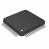
MAX5632UCB+D Maxim Integrated Products, MAX5632UCB+D Datasheet - Page 10

MAX5632UCB+D
Manufacturer Part Number
MAX5632UCB+D
Description
IC DAC 16BIT 32CH S&H 64-TQFP
Manufacturer
Maxim Integrated Products
Datasheet
1.MAX5633UCBD.pdf
(16 pages)
Specifications of MAX5632UCB+D
Number Of Bits
16
Data Interface
Serial
Number Of Converters
32
Voltage Supply Source
Dual ±
Operating Temperature
0°C ~ 85°C
Mounting Type
Surface Mount
Package / Case
64-LQFP
Lead Free Status / RoHS Status
Lead free / RoHS Compliant
Power Dissipation (max)
-
Settling Time
-
16-Bit DACs with 32-Channel
Sample-and-Hold Outputs
voltage at the ground-sense input. With a 2.5V refer-
ence, the nominal endpoints are -4.0535V and
+9.0535V (Table 1). Note that these are “virtual” inter-
nal endpoint voltages and cannot be reached with all
combinations of negative and positive power-supply
voltages. The nominal, useable DAC endpoint codes
for the selected power supplies may be calculated as:
The resistive voltage-divider formed by the output resis-
tor (R
put voltage. Determine V
Figure 4. Input Word Sequence
10
Figure 3. Analog Block Diagram
D15 D14 D13 D12 D11 D10 D09 D08 D07 D06 D05 D04 D03 D02 D01
lower endpoint code = 32768 - ((2.5V - (V
MSB
upper endpoint code = 32768 + ((V
______________________________________________________________________________________
O
) and the load impedance (R
Scaling Factor
V
OUT
_
200µV) (result ≤ 65535)
=
DATA
200µV) (result ≥ 0)
V
DAC
GS
V
REF
CHOLD
OUT_
=
R
16-BIT
×
DAC
L
scaling factor
as follows:
R
+
L
R
O
DATA
L
DD
), scales the out-
- 2.4 - 2.5V) /
SS
OFFSET
GAIN
AND
+ 0.75) /
C
The MAX5631/MAX5632/MAX5633 include a ground-
sense input (GS), which allows the output voltages to
be referenced to a remote ground. The voltage at GS is
added to the output voltage with unity gain. Note that
the resulting output voltage must be within the valid
output voltage range set by the power supplies.
The MAX5631/MAX5632/MAX5633 clamps the output
between two externally applied voltages. Internal
diodes at each channel restrict the output voltage to:
The clamping diodes allow the MAX5631/MAX5632/
MAX5633 to drive devices with restricted input ranges.
The diodes also allow the outputs to be clamped during
power-up or fault conditions. To disable output clamp-
ing, connect CH to V
clamping voltages beyond the maximum output voltage
range.
The MAX5631/MAX5632/MAX5633 are controlled by an
SPI, QSPI, and MICROWIRE-compatible 3-wire inter-
face. Serial data is clocked into the 24-bit shift register
in an MSB-first format, with the 16-bit DAC data pre-
ceding the 5-bit SRAM address, 2-bit control, and a fill
0 (Figure 4). The input word is framed by CS. The first
HOLD
ONE OF 32 SHA CHANNELS
A
V
(
V
= 1
CH
D0
+
0 7
R
.
O
A4
V
)
≥
DD
A3
V
ADDRESS
OUT
and CL to V
A2
CH
CL
_
R
≥
L
OUT_
(
A1
V
CL
Serial Interface
Ground Sense
−
A0
Output Clamp
0 7
.
SS
V
C1
, setting the
)
CONTROL
C0
LSB
0


