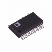
AD5554BRS Analog Devices Inc, AD5554BRS Datasheet - Page 12

AD5554BRS
Manufacturer Part Number
AD5554BRS
Description
IC DAC 14BIT QUAD SERIAL 28-SSOP
Manufacturer
Analog Devices Inc
Datasheet
1.AD5554BRSZ.pdf
(16 pages)
Specifications of AD5554BRS
Rohs Status
RoHS non-compliant
Settling Time
2µs
Number Of Bits
14
Data Interface
Serial
Number Of Converters
4
Voltage Supply Source
Dual ±
Power Dissipation (max)
1.25mW
Operating Temperature
-40°C ~ 85°C
Mounting Type
Surface Mount
Package / Case
28-SSOP
Available stocks
Company
Part Number
Manufacturer
Quantity
Price
Part Number:
AD5554BRSZ
Manufacturer:
ADI/亚德诺
Quantity:
20 000
AD5544/AD5554
SERIAL DATA INTERFACE
The AD5544/AD5554 use a 3-wire ( CS , SDI, CLK), SPI-compatible
serial data interface. Serial data of the AD5544/AD5554 is clocked
into the serial input register in an 18-bit and 16-bit data-word
format, respectively. The MSB bits are loaded first.
the 18 data-word bits for the AD5544, and
16 data-word bits for the AD5554. Data is placed on the SDI pin
and clocked into the register on the positive clock edge of CLK,
subject to the data setup and data hold time requirements specified
in the interface timing specifications (see
Data can be clocked in only while the CS chip select pin is active
low. For the AD5544, only the last 18 bits clocked into the serial
register are interrogated when the CS pin returns to the logic high
state; extra data bits are ignored. For the AD5554, only the last
16 bits clocked into the serial register are interrogated when the
CS pin returns to the logic high state. Because most microcon-
trollers output serial data in 8-bit bytes, three right-justified data
bytes can be written to the AD5544. Keeping the CS line low
between the first, second, and third byte transfers results in a
successful serial register update.
Table 5. AD5544 Serial Input Register Data Format, Data Is Loaded in the MSB-First Format
MSB
B17
A1
1
Table 6. AD5554 Serial Input Register Data Format, Data Is Loaded in the MSB-First Format
MSB
B15
A1
1
Table 7. Address Decode
A1
0
0
1
1
Only the last 18 bits of data clocked into the serial register (address + data) are inspected when the positive edge of the CS line returns to logic high. At this point, an
internally generated load strobe transfers the serial register data contents (Bit D15 to Bit D0) to the decoded DAC input register address determined by Bit A1 and Bit A0.
Any extra bits clocked into the AD5544 shift register are ignored; only the last 18 bits clocked in are used. If double-buffered data is not needed, the LDAC pin can be
tied logic low to disable the DAC registers.
Only the last 16 bits of data clocked into the serial register (address + data) are inspected when the positive edge of the CS line returns to logic high. At this point, an
internally generated load strobe transfers the serial register data contents (Bit D13 to Bit D0) to the decoded DAC input register address determined by Bit A1 and Bit A0.
Any extra bits clocked into the AD5554 shift register are ignored; only the last 16 bits clocked in are used. If double-buffered data is not needed, the LDAC pin can be
tied logic low to disable the DAC registers.
B16
A0
B14
A0
B15
D15
B13
D13
B14
D14
B12
D12
A0
0
1
0
1
B13
D13
B11
D11
Table 1
Table 6
B12
D12
Table 5
and
B10
D10
defines the
B11
D11
Table 2
defines
B9
D9
Rev. D | Page 12 of 16
B10
D10
).
B8
D8
DAC Decoded
DAC A
DAC B
DAC C
DAC D
B9
D9
Similarly, two right-justified data bytes can be written to the
AD5554. Keeping the CS line low between the first and second
byte transfer results in a successful serial register update.
When the data is properly aligned in the shift register, the posi-
tive edge of the CS initiates the transfer of new data to the target
DAC register, determined by the decoding of Address Bit A1
and Address Bit A0. For the AD5544,
and
interface.
For the AD5554, Table 6, Table 7, Table 9, and Figure 4 define
the characteristics of the software serial interface. Figure 21 and
Figure 22 show the equivalent logic interface for the key digital
control pins for the AD5544. The AD5554 has a similar configu-
ration, except that it has 14 data bits. Two additional pins, RS and
MSB, provide hardware control over the preset function and
DAC register loading. If these functions are not needed, the RS
pin can be tied to logic high. The asynchronous input RS pin
forces all input and the DAC registers to either the zero-code
state (MSB = 0) or the half-scale state (MSB = 1).
B7
D7
B8
D8
Figure 3
D7
B7
B6
D6
define the characteristics of the software serial
B6
D6
B5
D5
D5
B5
1
1
B4
D4
D4
B4
B3
D3
B3
D3
Table 5 Table 7 Table 8
B2
D2
B2
D2
,
B1
D1
B1
D1
,
LSB
D0
B0
LSB
B0
D0
,


