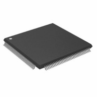
ADSP-2191MKSTZ-160 Analog Devices Inc, ADSP-2191MKSTZ-160 Datasheet - Page 11

ADSP-2191MKSTZ-160
Manufacturer Part Number
ADSP-2191MKSTZ-160
Description
IC DSP CONTROLLER 16BIT 144LQFP
Manufacturer
Analog Devices Inc
Series
ADSP-21xxr
Type
Fixed Pointr
Datasheet
1.ADSP-2191MKSTZ-160.pdf
(48 pages)
Specifications of ADSP-2191MKSTZ-160
Interface
Host Interface, SPI, SSP, UART
Clock Rate
160MHz
Non-volatile Memory
External
On-chip Ram
160kB
Voltage - I/o
3.00V, 3.30V
Voltage - Core
2.50V
Operating Temperature
0°C ~ 70°C
Mounting Type
Surface Mount
Package / Case
144-LQFP
No. Of Bits
16 Bit
Frequency
160MHz
Supply Voltage
3.3V
Embedded Interface Type
HPI, SPI, UART
No. Of I/o's
16
No. Of Mips
160
Lead Free Status / RoHS Status
Lead free / RoHS Compliant
Available stocks
Company
Part Number
Manufacturer
Quantity
Price
Company:
Part Number:
ADSP-2191MKSTZ-160
Manufacturer:
AD
Quantity:
1 000
Company:
Part Number:
ADSP-2191MKSTZ-160
Manufacturer:
Analog Devices Inc
Quantity:
10 000
Part Number:
ADSP-2191MKSTZ-160
Manufacturer:
ADI/亚德诺
Quantity:
20 000
Clock Signals
The ADSP-2191M can be clocked by a crystal oscillator or a
buffered, shaped clock derived from an external clock oscillator.
If a crystal oscillator is used, the crystal should be connected
across the CLKIN and XTAL pins, with two capacitors and a
1 MΩ shunt resistor connected as shown in
values are dependent on crystal type and should be specified by
the crystal manufacturer. A parallel-resonant, fundamental fre-
quency, microprocessor-grade crystal should be used for this
configuration.
If a buffered, shaped clock is used, this external clock connects
to the DSP’s CLKIN pin. CLKIN input cannot be halted,
changed, or operated below the specified frequency during
normal operation. When an external clock is used, the XTAL
input must be left unconnected.
The DSP provides a user-programmable 1 to 32 multiplica-
tion of the input clock, including some fractional values, to
support 128 external to internal (DSP core) clock ratios. The
MSEL6–0, BYPASS, and DF pins decide the PLL multiplication
factor at reset. At runtime, the multiplication factor can be con-
trolled in software. The combination of pullup and pull-down
resistors in
produces a 150 MHz core clock from the 25 MHz input. For
other clock multiplier settings, see the ADSP-219x/ADSP-2191
DSP Hardware Reference.
The peripheral clock is supplied to the CLKOUT pin.
All on-chip peripherals for the ADSP-2191M operate at the rate
set by the peripheral clock. The peripheral clock is either equal
to the core clock rate or one-half the DSP core clock rate. This
selection is controlled by the IOSEL bit in the PLLCTL register.
The maximum core clock is 160 MHz and the maximum periph-
eral clock is 80 MHz—the combination of the input clock and
core/peripheral clock ratios may not exceed these limits.
Reset
The RESET signal initiates a master reset of the ADSP-2191M.
The RESET signal must be asserted during the powerup
sequence to assure proper initialization. RESET during initial
powerup must be held long enough to allow the internal clock to
stabilize.
The powerup sequence is defined as the total time required for
the crystal oscillator circuit to stabilize after a valid V
to the processor, and for the internal phase-locked loop (PLL) to
lock onto the specific crystal frequency. A minimum of 100 µs
ensures that the PLL has locked, but does not include the crystal
oscillator start-up time. During this powerup sequence the
RESET signal should be held low. On any subsequent resets, the
RESET signal must meet the minimum pulsewidth specifica-
tion, t
The RESET input contains some hysteresis. If using an RC
circuit to generate your RESET signal, the circuit should use an
external Schmidt trigger.
REV. A
WRST
.
Figure 3
sets up a core clock ratio of 6:1, which
Figure
3. Capacitor
DD
is applied
–11–
The master reset sets all internal stack pointers to the empty stack
condition, masks all interrupts, and resets all registers to their
default values (where applicable). When RESET is released, if
there is no pending bus request and the chip is configured for
booting, the boot-loading sequence is performed. Program
control jumps to the location of the on-chip boot ROM
(0xFF 0000).
Power Supplies
The ADSP-2191M has separate power supply connections for
the internal (V
internal supply must meet the 2.5 V requirement. The external
supply must be connected to a 3.3 V supply. All external supply
pins must be connected to the same supply.
Power-Up Sequence
Power up together the two supplies V
cannot be powered up together, power up the internal (core)
supply first (powering up the core supply first reduces the risk of
latchup events.
Booting Modes
The ADSP-2191M has five mechanisms (listed in
automatically loading internal program memory after reset. Two
no-boot modes are also supported.
RUNTIME
PF PIN I/O
RESET
SOURCE
V
V
DD
DD
Figure 3. External Crystal Connections
DDINT
) and external (V
MSEL0 (PF0)
MSEL1 (PF1)
MSEL2 (PF2)
MSEL3 (PF3)
MSEL4 (PF4)
MSEL5 (PF5)
MSEL6 (PF6)
DF (PF7)
BYPASS
RESET
CLKIN
25MHz
1M
XTAL
ADSP-2196M
ADSP-2191M
DDEXT
DDEXT
CLKOUT
THE PULL-UP/PULL-DOWN
RESISTORS ON THE MSEL,
DF, AND BYPASS PINS
SELECT THE CORE CLOCK
RATIO.
HERE, THE SELECTION (6:1)
AND 25MHz INPUT CLOCK
PRODUCE A 150MHz CORE
CLOCK.
) power supplies. The
and V
DDINT
Table
. If they
6) for


