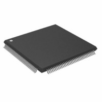
ADSP-2191MKSTZ-160 Analog Devices Inc, ADSP-2191MKSTZ-160 Datasheet - Page 15

ADSP-2191MKSTZ-160
Manufacturer Part Number
ADSP-2191MKSTZ-160
Description
IC DSP CONTROLLER 16BIT 144LQFP
Manufacturer
Analog Devices Inc
Series
ADSP-21xxr
Type
Fixed Pointr
Datasheet
1.ADSP-2191MKSTZ-160.pdf
(48 pages)
Specifications of ADSP-2191MKSTZ-160
Interface
Host Interface, SPI, SSP, UART
Clock Rate
160MHz
Non-volatile Memory
External
On-chip Ram
160kB
Voltage - I/o
3.00V, 3.30V
Voltage - Core
2.50V
Operating Temperature
0°C ~ 70°C
Mounting Type
Surface Mount
Package / Case
144-LQFP
No. Of Bits
16 Bit
Frequency
160MHz
Supply Voltage
3.3V
Embedded Interface Type
HPI, SPI, UART
No. Of I/o's
16
No. Of Mips
160
Lead Free Status / RoHS Status
Lead free / RoHS Compliant
Available stocks
Company
Part Number
Manufacturer
Quantity
Price
Company:
Part Number:
ADSP-2191MKSTZ-160
Manufacturer:
AD
Quantity:
1 000
Company:
Part Number:
ADSP-2191MKSTZ-160
Manufacturer:
Analog Devices Inc
Quantity:
10 000
Part Number:
ADSP-2191MKSTZ-160
Manufacturer:
ADI/亚德诺
Quantity:
20 000
Design-for-Emulation Circuit Information
For details on target board design issues including: single
processor connections, multiprocessor scan chains, signal buff-
ering, signal termination, and emulator pod logic, see the EE-68:
Analog Devices JTAG Emulation Technical Reference on the Analog
Devices website (www.analog.com)—use site search on
“EE-68.” This document is updated regularly to keep pace with
improvements to emulator support.
Table 7. Pin Function Descriptions
REV. A
Pin
A21–0
D7–0
D15
D14
D13
D12
D11
D10
D9
D8
PF7
PF6
/PF15
/SPI1SEL7
/PF14
/SPI0SEL7
/PF12
/SPI1SEL6
/PF12
/SPI0SEL6
/PF11
/SPI1SEL5
/PF10
/SPI0SEL5
/PF9
/SPI1SEL4
/PF8
/SPI0SEL4
/SPI1SEL3
/DF
/SPI0SEL3
/MSEL6
Figure 7. JTAG Pod Connector Keep-Out Area
0.15"
Type
O/T
I/O/T
I/O/T
I/O
I
I/O/T
I/O
I
I/O/T
I/O
I
I/O/T
I/O
I
I/O/T
I/O
I
I/O/T
I/O
I
I/O/T
I/O
I
I/O/T
I/O
I
I/O/T
I
I
I/O/T
I
I
Function
External Port Address Bus
External Port Data Bus, least significant 8 bits
Data 15 (if 16-bit external bus)/Programmable Flags 15 (if 8-bit external bus)/SPI1 Slave
Select output 7 (if 8-bit external bus, when SPI1 enabled)
Data 14 (if 16-bit external bus)/Programmable Flags 14 (if 8-bit external bus)/SPI0 Slave
Select output 7 (if 8-bit external bus, when SPI0 enabled)
Data 13 (if 16-bit external bus)/Programmable Flags 13 (if 8-bit external bus)/SPI1 Slave
Select output 6 (if 8-bit external bus, when SPI1 enabled)
Data 12 (if 16-bit external bus)/Programmable Flags 12 (if 8-bit external bus)/SPI0 Slave
Select output 6 (if 8-bit external bus, when SPI0 enabled)
Data 11 (if 16-bit external bus)/Programmable Flags 11 (if 8-bit external bus)/SPI1 Slave
Select output 5 (if 8-bit external bus, when SPI1 enabled)
Data 10 (if 16-bit external bus)/Programmable Flags 10 (if 8-bit external bus)/SPI0 Slave
Select output 5 (if 8-bit external bus, when SPI0 enabled)
Data 9 (if 16-bit external bus)/Programmable Flags 9 (if 8-bit external bus)/SPI1 Slave Select
output 4 (if 8-bit external bus, when SPI1 enabled)
Data 8 (if 16-bit external bus)/Programmable Flags 8 (if 8-bit external bus)/SPI0 Slave Select
output 4 (if 8-bit external bus, when SPI0 enabled)
Programmable Flags 7/SPI1 Slave Select output 3 (when SPI0 enabled)/Divisor Frequency
(divisor select for PLL input during boot)
Programmable Flags 6/SPI0 Slave Select output 3 (when SPI0 enabled)/Multiplier Select 6
(during boot)
0.10"
–15–
Additional Information
This data sheet provides a general overview of the ADSP-2191M
architecture and functionality. For detailed information on the
core architecture of the ADSP-219x family, refer to the
ADSP-219x/ADSP-2191 DSP Hardware Reference. For details on
the instruction set, refer to the ADSP-219x Instruction Set
Reference.
PIN FUNCTION DESCRIPTIONS
ADSP-2191M pin definitions are listed in
ADSP-2191M inputs are asynchronous and can be asserted
asynchronously to CLKIN (or to TCK for TRST).
Tie or pull unused inputs to V
ADDR21–0, DATA15–0, PF7-0, and inputs that have internal
pull-up or pull-down resistors (TRST, BMODE0, BMODE1,
OPMODE, BYPASS, TCK, TMS, TDI, and RESET)—these
pins can be left floating. These pins have a logic-level hold circuit
that prevents input from floating internally.
The following symbols appear in the Type column of
= Ground, I = Input, O = Output, P = Power Supply, and T =
Three-State.
DDEXT
ADSP-2191M
or GND, except for
Table
7. All
Table
7: G


