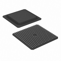
XC3S500E-4FGG320I Xilinx Inc, XC3S500E-4FGG320I Datasheet - Page 173

XC3S500E-4FGG320I
Manufacturer Part Number
XC3S500E-4FGG320I
Description
IC FPGA SPARTAN-3E 500K 320-FBGA
Manufacturer
Xilinx Inc
Series
Spartan™-3Er
Datasheet
1.XC3S100E-4VQG100C.pdf
(233 pages)
Specifications of XC3S500E-4FGG320I
Number Of Logic Elements/cells
10476
Number Of Labs/clbs
1164
Total Ram Bits
368640
Number Of I /o
232
Number Of Gates
500000
Voltage - Supply
1.14 V ~ 1.26 V
Mounting Type
Surface Mount
Operating Temperature
-40°C ~ 100°C
Package / Case
320-BGA
For Use With
122-1536 - KIT STARTER SPARTAN-3E
Lead Free Status / RoHS Status
Lead free / RoHS Compliant
Available stocks
Company
Part Number
Manufacturer
Quantity
Price
Company:
Part Number:
XC3S500E-4FGG320I
Manufacturer:
SILICON
Quantity:
2 300
Company:
Part Number:
XC3S500E-4FGG320I
Manufacturer:
XILINX
Quantity:
8
Company:
Part Number:
XC3S500E-4FGG320I
Manufacturer:
Xilinx Inc
Quantity:
10 000
Part Number:
XC3S500E-4FGG320I
Manufacturer:
XILINX/赛灵思
Quantity:
20 000
- Current page: 173 of 233
- Download datasheet (6Mb)
CP132: 132-ball Chip-scale Package
The XC3S100E, XC3S250E and the XC3S500E FPGAs
are available in the 132-ball chip-scale package, CP132.
The devices share a common footprint for this package as
shown in
Table 133
by bank number and then by pin name. Pins that form a dif-
ferential I/O pair appear together in the table. The table also
shows the pin number for each pin and the pin type, as
defined earlier.
Physically, the D14 and K2 balls on the XC3S100E and
XC3S250E FPGAs are not connected but should be con-
Pinout Table
Table 133: CP132 Package Pinout
DS312-4 (v3.8) August 26, 2009
Product Specification
Bank
0
0
0
0
0
0
0
0
0
0
0
0
0
0
0
0
0
0
0
0
0
0
Table 133
lists all the CP132 package pins. They are sorted
R
IO_L01N_0
IO_L01P_0
N.C. ( )
N.C. ( )
N.C. ( )
IP
IO_L04N_0/GCLK5
IO_L04P_0/GCLK4
IO_L05N_0/GCLK7
IO_L05P_0/GCLK6
IO_L07N_0/GCLK11
IO_L07P_0/GCLK10
IO_L08N_0/VREF_0
IO_L08P_0
IO_L09N_0
IO_L09P_0
N.C. ( )
IP
IO_L11N_0/HSWAP
IO_L11P_0
IP_L06N_0/GCLK9
IP_L06P_0/GCLK8
and
Figure
XC3S100E
Pin Name
82.
IO_L01N_0
IO_L01P_0
IO_L04N_0/GCLK5
IO_L05N_0/GCLK7
IO_L05P_0/GCLK6
IP_L06P_0/GCLK8
IO_L02N_0
IO_L02P_0
IO_L03N_0/VREF_0
IO_L03P_0
IO_L04P_0/GCLK4
IO_L07N_0/GCLK11
IO_L07P_0/GCLK10
IO_L08N_0/VREF_0
IO_L08P_0
IO_L09N_0
IO_L09P_0
IO_L10N_0
IO_L10P_0
IO_L11N_0/HSWAP
IO_L11P_0
IP_L06N_0/GCLK9
www.xilinx.com
nected to VCCINT to maintain density migration compatibil-
ity.
Similarly, the A4, C1, and P10 balls on the XC3S100E
FPGA are not connected but should be connected to GND
to maintain density migration compatibility.
The XC3S100E FPGA has four fewer BPI address pins,
A[19:0], whereas the XC3S250E and XC3S500E support
A[23:0].
An electronic version of this package pinout table and foot-
print diagram is available for download from the Xilinx web
site at:
http://www.xilinx.com/support/documentation/data_sheets/s3e_pin.zip
XC3S250E
XC3S500E
Pin Name
CP132 Ball
C12
C11
A13
A12
B12
B11
A10
C9
C6
A9
B9
B7
A7
B6
C5
B5
C4
B4
B3
A3
C8
B8
Pinout Descriptions
Others: VREF (I/O)
100E: INPUT
100E: INPUT
Others: I/O
Others: I/O
Others: I/O
Others: I/O
Others: I/O
100E: N.C.
100E: N.C.
100E: N.C.
100E: N.C.
GCLK
GCLK
GCLK
GCLK
GCLK
GCLK
VREF
GCLK
GCLK
DUAL
Type
I/O
I/O
I/O
I/O
I/O
I/O
173
Related parts for XC3S500E-4FGG320I
Image
Part Number
Description
Manufacturer
Datasheet
Request
R

Part Number:
Description:
IC SPARTAN-3E FPGA 500K 320FBGA
Manufacturer:
Xilinx Inc
Datasheet:

Part Number:
Description:
IC FPGA SPARTAN-3E 500K 208-PQFP
Manufacturer:
Xilinx Inc
Datasheet:

Part Number:
Description:
IC FPGA SPARTAN-3E 500K 132CSBGA
Manufacturer:
Xilinx Inc
Datasheet:

Part Number:
Description:
IC FPGA SPARTAN-3E 500K 256FTBGA
Manufacturer:
Xilinx Inc
Datasheet:

Part Number:
Description:
IC FPGA SPARTAN-3E 500K 256FTBGA
Manufacturer:
Xilinx Inc
Datasheet:

Part Number:
Description:
IC FPGA SPARTAN 3E 320FBGA
Manufacturer:
Xilinx Inc
Datasheet:

Part Number:
Description:
FPGA Spartan®-3E Family 500K Gates 10476 Cells 572MHz 90nm (CMOS) Technology 1.2V 256-Pin FTBGA
Manufacturer:
Xilinx Inc
Datasheet:

Part Number:
Description:
FPGA Spartan®-3E Family 500K Gates 10476 Cells 572MHz 90nm (CMOS) Technology 1.2V 208-Pin PQFP
Manufacturer:
Xilinx Inc
Datasheet:

Part Number:
Description:
FPGA Spartan®-3E Family 500K Gates 10476 Cells 572MHz 90nm (CMOS) Technology 1.2V 208-Pin PQFP
Manufacturer:
Xilinx Inc
Datasheet:

Part Number:
Description:
FPGA Spartan®-3E Family 500K Gates 10476 Cells 572MHz 90nm (CMOS) Technology 1.2V 256-Pin FTBGA
Manufacturer:
Xilinx Inc
Datasheet:

Part Number:
Description:
FPGA Spartan®-3E Family 500K Gates 10476 Cells 572MHz 90nm (CMOS) Technology 1.2V 132-Pin CSBGA
Manufacturer:
Xilinx Inc
Datasheet:

Part Number:
Description:
FPGA Spartan-3E Family 500K Gates 10476 Cells 572MHz 90nm (CMOS) Technology 1.2V 320-Pin FBGA
Manufacturer:
Xilinx Inc
Datasheet:

Part Number:
Description:
IC FPGA SPARTAN-3E 500K 100-VQFP
Manufacturer:
Xilinx Inc
Datasheet:

Part Number:
Description:
IC FPGA SPARTAN-3E 500K 132CSBGA
Manufacturer:
Xilinx Inc
Datasheet:

Part Number:
Description:
IC FPGA SPARTAN-3E 500K 320-FBGA
Manufacturer:
Xilinx Inc
Datasheet:


