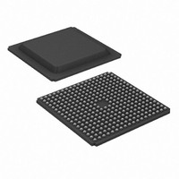
XC3S500E-4FGG320I Xilinx Inc, XC3S500E-4FGG320I Datasheet - Page 33

XC3S500E-4FGG320I
Manufacturer Part Number
XC3S500E-4FGG320I
Description
IC FPGA SPARTAN-3E 500K 320-FBGA
Manufacturer
Xilinx Inc
Series
Spartan™-3Er
Datasheet
1.XC3S100E-4VQG100C.pdf
(233 pages)
Specifications of XC3S500E-4FGG320I
Number Of Logic Elements/cells
10476
Number Of Labs/clbs
1164
Total Ram Bits
368640
Number Of I /o
232
Number Of Gates
500000
Voltage - Supply
1.14 V ~ 1.26 V
Mounting Type
Surface Mount
Operating Temperature
-40°C ~ 100°C
Package / Case
320-BGA
For Use With
122-1536 - KIT STARTER SPARTAN-3E
Lead Free Status / RoHS Status
Lead free / RoHS Compliant
Available stocks
Company
Part Number
Manufacturer
Quantity
Price
Company:
Part Number:
XC3S500E-4FGG320I
Manufacturer:
SILICON
Quantity:
2 300
Company:
Part Number:
XC3S500E-4FGG320I
Manufacturer:
XILINX
Quantity:
8
Company:
Part Number:
XC3S500E-4FGG320I
Manufacturer:
Xilinx Inc
Quantity:
10 000
Part Number:
XC3S500E-4FGG320I
Manufacturer:
XILINX/赛灵思
Quantity:
20 000
- Current page: 33 of 233
- Download datasheet (6Mb)
Table 18: Dual-Port RAM Function
DS312-2 (v3.8) August 26, 2009
Product Specification
Notes:
1.
2.
WE (mode)
1 (write)
0 (read)
1 (read)
1 (read)
1 (read)
data_a = word addressed by bits A3-A0.
data_d = word addressed by bits DPRA3-DPRA0.
Figure 27: Dual-Port RAM Component
R
Inputs
WCLK
DPRA0
DPRA1
DPRA2
DPRA3
WCLK
↑
X
0
1
↓
WE
A0
A1
A2
A3
D
DPRA[3:0]
RAM16X1D
WCLK
A[3:0]
D
X
X
X
D
X
WE
D
DS312-2_42_021305
SPO
DPO
data_a
data_a
data_a
data_a
SPO
D
Figure 26: RAM16X1D Dual-Port Usage
Outputs
data_d
data_d
data_d
data_d
data_d
DPO
www.xilinx.com
(Read/
Write)
RAM
(Read
16x1
RAM
16x1
Only)
LUT
LUT
Table 19: Distributed RAM Signals
WCLK
WE
A0, A1, A2,
A3 (A4, A5)
D
O, SPO, and
DPO
SLICEM
Signal
Optional
Register
Optional
Register
The clock is used for synchronous writes.
The data and the address input pins have
setup times referenced to the WCLK pin.
Active on the positive edge by default
with built-in programmable polarity.
The enable pin affects the write
functionality of the port. An inactive Write
Enable prevents any writing to memory
cells. An active Write Enable causes the
clock edge to write the data input signal
to the memory location pointed to by the
address inputs. Active High by default
with built-in programmable polarity.
The address inputs select the memory
cells for read or write. The width of the
port determines the required address
inputs.
The data input provides the new data
value to be written into the RAM.
The data output O on single-port RAM or
the SPO and DPO outputs on dual-port
RAM reflects the contents of the memory
cells referenced by the address inputs.
Following an active write clock edge, the
data out (O or SPO) reflects the newly
written data.
DS312-2_41_021305
SPO
DPO
Description
Functional Description
33
Related parts for XC3S500E-4FGG320I
Image
Part Number
Description
Manufacturer
Datasheet
Request
R

Part Number:
Description:
IC SPARTAN-3E FPGA 500K 320FBGA
Manufacturer:
Xilinx Inc
Datasheet:

Part Number:
Description:
IC FPGA SPARTAN-3E 500K 208-PQFP
Manufacturer:
Xilinx Inc
Datasheet:

Part Number:
Description:
IC FPGA SPARTAN-3E 500K 132CSBGA
Manufacturer:
Xilinx Inc
Datasheet:

Part Number:
Description:
IC FPGA SPARTAN-3E 500K 256FTBGA
Manufacturer:
Xilinx Inc
Datasheet:

Part Number:
Description:
IC FPGA SPARTAN-3E 500K 256FTBGA
Manufacturer:
Xilinx Inc
Datasheet:

Part Number:
Description:
IC FPGA SPARTAN 3E 320FBGA
Manufacturer:
Xilinx Inc
Datasheet:

Part Number:
Description:
FPGA Spartan®-3E Family 500K Gates 10476 Cells 572MHz 90nm (CMOS) Technology 1.2V 256-Pin FTBGA
Manufacturer:
Xilinx Inc
Datasheet:

Part Number:
Description:
FPGA Spartan®-3E Family 500K Gates 10476 Cells 572MHz 90nm (CMOS) Technology 1.2V 208-Pin PQFP
Manufacturer:
Xilinx Inc
Datasheet:

Part Number:
Description:
FPGA Spartan®-3E Family 500K Gates 10476 Cells 572MHz 90nm (CMOS) Technology 1.2V 208-Pin PQFP
Manufacturer:
Xilinx Inc
Datasheet:

Part Number:
Description:
FPGA Spartan®-3E Family 500K Gates 10476 Cells 572MHz 90nm (CMOS) Technology 1.2V 256-Pin FTBGA
Manufacturer:
Xilinx Inc
Datasheet:

Part Number:
Description:
FPGA Spartan®-3E Family 500K Gates 10476 Cells 572MHz 90nm (CMOS) Technology 1.2V 132-Pin CSBGA
Manufacturer:
Xilinx Inc
Datasheet:

Part Number:
Description:
FPGA Spartan-3E Family 500K Gates 10476 Cells 572MHz 90nm (CMOS) Technology 1.2V 320-Pin FBGA
Manufacturer:
Xilinx Inc
Datasheet:

Part Number:
Description:
IC FPGA SPARTAN-3E 500K 100-VQFP
Manufacturer:
Xilinx Inc
Datasheet:

Part Number:
Description:
IC FPGA SPARTAN-3E 500K 132CSBGA
Manufacturer:
Xilinx Inc
Datasheet:

Part Number:
Description:
IC FPGA SPARTAN-3E 500K 320-FBGA
Manufacturer:
Xilinx Inc
Datasheet:


