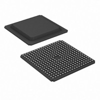
XC3S400-4FG320I Xilinx Inc, XC3S400-4FG320I Datasheet - Page 27

XC3S400-4FG320I
Manufacturer Part Number
XC3S400-4FG320I
Description
IC SPARTAN-3 FPGA 400K 320-FBGA
Manufacturer
Xilinx Inc
Series
Spartan™-3r
Datasheet
1.XC3S50-4VQG100C.pdf
(217 pages)
Specifications of XC3S400-4FG320I
Number Of Logic Elements/cells
8064
Number Of Labs/clbs
896
Total Ram Bits
294912
Number Of I /o
221
Number Of Gates
400000
Voltage - Supply
1.14 V ~ 1.26 V
Mounting Type
Surface Mount
Operating Temperature
-40°C ~ 100°C
Package / Case
320-BGA
Other names
Q3365683
Available stocks
Company
Part Number
Manufacturer
Quantity
Price
- Current page: 27 of 217
- Download datasheet (6Mb)
Table 12: Block RAM Port Signals (Continued)
DS099-2 (v2.5) December 4, 2009
Product Specification
Data Output
Bus
Parity Data
Output(s)
Write Enable
Clock Enable
Set/Reset
Clock
Description
Signal
R
Port A
Signal
Name
DOPA
SSRA
CLKA
WEA
DOA
ENA
Port B
Signal
DOPB
Name
SSRB
CLKB
WEB
DOB
ENB
Direction
Output
Output
Input
Input
Input
Input
www.xilinx.com
Basic data access occurs whenever WE is inactive. The DO
outputs mirror the data stored in the addressed memory
location.
Data access with WE asserted is also possible if one of the
following two attributes is chosen: WRITE_FIRST and
READ_FIRST. WRITE_FIRST simultaneously presents the new
input data on the DO output port and writes the data to the
address RAM location. READ_FIRST presents the previously
stored RAM data on the DO output port while writing new data
to RAM.
A third attribute, NO_CHANGE, latches the DO outputs upon
the assertion of WE.
It is possible to configure a port’s total data path width (w) to be
1, 2, 4, 9, 18, or 36 bits. This selection applies to both the DI and
DO paths. See the DI signal description.
Parity inputs represent additional bits included in the data input
path to support error detection. The number of parity bits "p"
included in the DI (same as for the DO bus) depends on a port’s
total data path width (w). See
When asserted together with EN, this input enables the writing
of data to the RAM. In this case, the data access attributes
WRITE_FIRST, READ_FIRST or NO_CHANGE determines if
and how data is updated on the DO outputs. See the DO signal
description.
When WE is inactive with EN asserted, read operations are still
possible. In this case, a transparent latch passes data from the
addressed memory location to the DO outputs.
When asserted, this input enables the CLK signal to
synchronize Block RAM functions as follows: the writing of data
to the DI inputs (when WE is also asserted), the updating of data
at the DO outputs as well as the setting/resetting of the DO
output latches.
When de-asserted, the above functions are disabled.
When asserted, this pin forces the DO output latch to the value
that the SRVAL attribute is set to. A Set/Reset operation on one
port has no effect on the other ports functioning, nor does it
disturb the memory’s data contents. It is synchronized to the
CLK signal.
This input accepts the clock signal to which read and write
operations are synchronized. All associated port inputs are
required to meet setup times with respect to the clock signal’s
active edge. The data output bus responds after a clock-to-out
delay referenced to the clock signal’s active edge.
Spartan-3 FPGA Family: Functional Description
Function
Table
13.
27
Related parts for XC3S400-4FG320I
Image
Part Number
Description
Manufacturer
Datasheet
Request
R

Part Number:
Description:
IC SPARTAN-3 FPGA 400K 208PQFP
Manufacturer:
Xilinx Inc
Datasheet:

Part Number:
Description:
SPARTAN-3A FPGA 400K 208-PQFP
Manufacturer:
Xilinx Inc
Datasheet:

Part Number:
Description:
SPARTAN-3A FPGA 400K 256-FTBGA
Manufacturer:
Xilinx Inc
Datasheet:

Part Number:
Description:
SPARTAN3A FPGA 400K STD 256FTBGA
Manufacturer:
Xilinx Inc

Part Number:
Description:
SEMI CONDUCTOR
Manufacturer:
Xilinx Inc
Datasheet:

Part Number:
Description:
FPGA Spartan®-3 Family 400K Gates 8064 Cells 630MHz 90nm Technology 1.2V 456-Pin FBGA
Manufacturer:
Xilinx Inc
Datasheet:

Part Number:
Description:
FPGA Spartan®-3 Family 400K Gates 8064 Cells 630MHz 90nm Technology 1.2V 320-Pin FBGA
Manufacturer:
Xilinx Inc
Datasheet:

Part Number:
Description:
FPGA Spartan®-3 Family 400K Gates 8064 Cells 630MHz 90nm Technology 1.2V 456-Pin FBGA
Manufacturer:
Xilinx Inc
Datasheet:

Part Number:
Description:
FPGA Spartan®-3 Family 400K Gates 8064 Cells 630MHz 90nm Technology 1.2V 256-Pin FTBGA
Manufacturer:
Xilinx Inc
Datasheet:

Part Number:
Description:
FPGA Spartan®-3 Family 400K Gates 8064 Cells 630MHz 90nm Technology 1.2V 208-Pin PQFP
Manufacturer:
Xilinx Inc
Datasheet:

Part Number:
Description:
FPGA Spartan®-3 Family 400K Gates 8064 Cells 630MHz 90nm Technology 1.2V 144-Pin TQFP
Manufacturer:
Xilinx Inc
Datasheet:

Part Number:
Description:
FPGA Spartan®-3 Family 400K Gates 8064 Cells 630MHz 90nm Technology 1.2V 144-Pin TQFP
Manufacturer:
Xilinx Inc
Datasheet:

Part Number:
Description:
FPGA Spartan®-3 Family 400K Gates 8064 Cells 725MHz 90nm Technology 1.2V 256-Pin FTBGA
Manufacturer:
Xilinx Inc
Datasheet:

Part Number:
Description:
FPGA Spartan®-3 Family 400K Gates 8064 Cells 630MHz 90nm Technology 1.2V 456-Pin FBGA
Manufacturer:
Xilinx Inc
Datasheet:

Part Number:
Description:
FPGA Spartan®-3 Family 400K Gates 8064 Cells 630MHz 90nm Technology 1.2V 320-Pin FBGA
Manufacturer:
Xilinx Inc
Datasheet:


