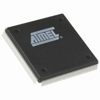
AT40K40-2EQI Atmel, AT40K40-2EQI Datasheet - Page 11

AT40K40-2EQI
Manufacturer Part Number
AT40K40-2EQI
Description
IC FPGA 40K GATES 240PQFP
Manufacturer
Atmel
Series
AT40K/KLVr
Specifications of AT40K40-2EQI
Number Of Logic Elements/cells
2304
Total Ram Bits
18432
Number Of I /o
193
Number Of Gates
50000
Voltage - Supply
4.5 V ~ 5.5 V
Mounting Type
Surface Mount
Operating Temperature
-40°C ~ 85°C
Package / Case
240-BFQFP
Lead Free Status / RoHS Status
Contains lead / RoHS non-compliant
Number Of Labs/clbs
-
Other names
AT40K402EQI
RAM
0896C–FPGA–04/02
32 x 4 dual-ported RAM blocks are dispersed throughout the array, see Figure 7. A 4-bit
Input Data Bus connects to four horizontal local buses distributed over four sector rows
(plane 1). A 4-bit Output Data Bus connects to four horizontal local buses distributed
over four sectors in the same column. A 5-bit Output Address Bus connects to five verti-
cal express buses in the same column. Ain (input address) and Aout (output address)
alternate positions in horizontally aligned RAM blocks. For the left-most RAM blocks,
Aout is on the left and Ain is on the right. For the right-most RAM blocks, Ain is on the
left and Aout is tied off, thus it can only be configured as a single port. For single-ported
RAM, Ain is the READ/WRITE address port and Din is the (bi-directional) data port.
Right-most RAM blocks can be used only for single-ported memories. WEN and OEN
connect to the vertical express buses in the same column.
Figure 7. RAM Connections (One Ram Block)
AT40K/AT40KLV Series FPGA
CLK
CLK
CLK
CLK
Ain
WEN
OEN
32 x 4 RAM
Din
CLK
Dout
Aout
11


