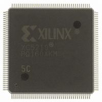
XC5210-5PQ160C Xilinx Inc, XC5210-5PQ160C Datasheet - Page 14

XC5210-5PQ160C
Manufacturer Part Number
XC5210-5PQ160C
Description
IC FPGA 324 CLB'S 160-PQFP
Manufacturer
Xilinx Inc
Series
XC5200r
Datasheet
1.XC5206-5PQ208C.pdf
(73 pages)
Specifications of XC5210-5PQ160C
Number Of Logic Elements/cells
1296
Number Of Labs/clbs
324
Number Of I /o
133
Number Of Gates
16000
Voltage - Supply
4.75 V ~ 5.25 V
Mounting Type
Surface Mount
Operating Temperature
0°C ~ 85°C
Package / Case
160-BQFP
Lead Free Status / RoHS Status
Contains lead / RoHS non-compliant
Total Ram Bits
-
Other names
122-1146
Available stocks
Company
Part Number
Manufacturer
Quantity
Price
XC5200 Series Field Programmable Gate Arrays
Two low-skew horizontal and vertical unidirectional glo-
bal-line segments span each row and column of the chip,
respectively.
Single- and Double-Length Lines
The single- and double-length bidirectional line segments
make up the bulk of the routing channels. The dou-
ble-length lines hop across every other CLB to reduce the
propagation delays in speed-critical nets. Regenerating the
signal strength is recommended after traversing three or
four such segments. Xilinx place-and-route software auto-
matically connects buffers in the path of the signal as nec-
essary. Single- and double-length lines cannot drive onto
Longlines and global lines; Longlines and global lines can,
however, drive onto single- and double-length lines. As a
general rule, Longline and global-line connections to the
general routing matrix are unidirectional, with the signal
direction from these lines toward the routing matrix.
Longlines
Longlines are used for high-fan-out signals, 3-state busses,
low-skew nets, and faraway destinations. Row and column
splitter PIPs in the middle of the array effectively double the
total number of Longlines by electrically dividing them into
two separated half-lines. Longlines are driven by the
3-state buffers in each CLB, and are driven by similar buff-
ers at the periphery of the array from the VersaRing I/O
Interface.
Bus-oriented designs are easily implemented by using Lon-
glines in conjunction with the 3-state buffers in the CLB and
in the VersaRing. Additionally, weak keeper cells at the
periphery retain the last valid logic level on the Longlines
when all buffers are in 3-state mode.
Longlines connect to the single-length or double-length
lines, or to the logic inside the CLB, through the General
Routing Matrix. The only manner in which a Longline can
be driven is through the four 3-state buffers; therefore, a
Longline-to-Longline or single-line-to-Longline connection
through PIPs in the General Routing Matrix is not possible.
Again, as a general rule, long- and global-line connections
to the General Routing Matrix are unidirectional, with the
signal direction from these lines toward the routing matrix.
The XC5200 family has no pull-ups on the ends of the Lon-
glines sourced by TBUFs, unlike the XC4000 Series. Con-
sequently, wired functions (i.e., WAND and WORAND) and
wide multiplexing functions requiring pull-ups for undefined
states (i.e., bus applications) must be implemented in a dif-
ferent way. In the case of the wired functions, the same
functionality can be achieved by taking advantage of the
7-96
segments span the width and height of the chip,
respectively.
Product Obsolete or Under Obsolescence
carry/cascade logic described above, implementing a wide
logic function in place of the wired function. In the case of
3-state bus applications, the user must insure that all states
of the multiplexing function are defined. This process is as
simple as adding an additional TBUF to drive the bus High
when the previously undefined states are activated.
Global Lines
Global buffers in Xilinx FPGAs are special buffers that drive
a dedicated routing network called Global Lines, as shown
in
clocks or other control signals, to maximize speed and min-
imize skewing while distributing the signal to many loads.
The XC5200 family has a total of four global buffers (BUFG
symbol in the library), each with its own dedicated routing
channel. Two are distributed vertically and two horizontally
throughout the FPGA.
The global lines provide direct input only to the CLB clock
pins. The global lines also connect to the General Routing
Matrix to provide access from these lines to the function
generators and other control signals.
Four clock input pads at the corners of the chip, as shown
in
to each of the four global-line buffers. In addition to the ded-
icated pad, the global lines can be sourced by internal
logic. PIPs from several routing channels within the Ver-
saRing can also be configured to drive the global-line buff-
ers.
Details of all the programmable interconnect for a CLB is
shown in
Figure 16: Global Lines
Figure
GCK2
GCK1
Figure
16, provide a high-speed, low-skew clock network
Figure
16. This network is intended for high-fanout
17.
November 5, 1998 (Version 5.2)
GCK3
GCK4
X5704
R


