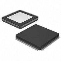
XC5210-6PQ208C Xilinx Inc, XC5210-6PQ208C Datasheet - Page 45

XC5210-6PQ208C
Manufacturer Part Number
XC5210-6PQ208C
Description
IC FPGA 324 CLB'S 208-PQFP
Manufacturer
Xilinx Inc
Series
XC5200r
Datasheet
1.XC5206-5PQ208C.pdf
(73 pages)
Specifications of XC5210-6PQ208C
Number Of Logic Elements/cells
1296
Number Of Labs/clbs
324
Number Of I /o
164
Number Of Gates
16000
Voltage - Supply
4.75 V ~ 5.25 V
Mounting Type
Surface Mount
Operating Temperature
0°C ~ 85°C
Package / Case
208-BFQFP
Lead Free Status / RoHS Status
Contains lead / RoHS non-compliant
Total Ram Bits
-
Other names
122-1149
Available stocks
Company
Part Number
Manufacturer
Quantity
Price
Company:
Part Number:
XC5210-6PQ208C
Manufacturer:
XILINX
Quantity:
88
Part Number:
XC5210-6PQ208C
Manufacturer:
XILINX/赛灵思
Quantity:
20 000
XC5200 Switching Characteristics
Definition of Terms
In the following tables, some specifications may be designated as Advance or Preliminary. These terms are defined as
follows:
Advance:
Preliminary: Based on preliminary characterization. Further changes are not expected.
Unmarked:
XC5200 Operating Conditions
XC5200 DC Characteristics Over Operating Conditions
XC5200 Absolute Maximum Ratings
1. Notwithstanding the definition of the above terms, all specifications are subject to change without notice.
November 5, 1998 (Version 5.2)
V
V
V
V
V
T
V
V
I
I
C
I
Note:
V
V
V
T
T
T
Note:
Symbol
Symbol
CCO
IL
RIN
STG
SOL
IN
OH
OL
J
CC
IHT
ILT
IHC
ILC
CC
IN
TS
IN
Symbol
Stresses beyond those listed under Absolute Maximum Ratings may cause permanent damage to the device. These are stress
ratings only, and functional operation of the device at these or any other conditions beyond those listed under Recommended
Operating Conditions is not implied. Exposure to Absolute Maximum Ratings conditions for extended periods of time may
affect device reliability.
1. With no output current loads, all package pins at Vcc or GND, either TTL or CMOS inputs, and the FPGA configured with a
Supply voltage relative to GND Commercial: 0 C to 85 C junction
Supply voltage relative to GND Industrial: -40 C to 100 C junction
High-level input voltage — TTL configuration
Low-level input voltage — TTL configuration
High-level input voltage — CMOS configuration
Low-level input voltage — CMOS configuration
Input signal transition time
High-level output voltage @ I
Low-level output voltage @ I
Quiescent FPGA supply current (Note 1)
Leakage current
Input capacitance (sample tested)
Pad pull-up (when selected) @ V
tie option.
Supply voltage relative to GND
Input voltage with respect to GND
Voltage applied to 3-state output
Storage temperature (ambient)
Maximum soldering temperature (10 s @ 1/16 in. = 1.5 mm)
Junction temperature in plastic packages
Junction temperature in ceramic packages
Specifications not identified as either Advance or Preliminary are to be considered Final.
families. Use as estimates, not for production.
R
Initial estimates based on simulation and/or extrapolation from other speed grades, devices, or device
Product Obsolete or Under Obsolescence
OL
OH
Description
= 8.0 mA, V
= -8.0 mA, V
IN
Description
Description
= 0V (sample tested)
CC
CC
max
min
XC5200 Series Field Programmable Gate Arrays
-0.5 to +7.0
-0.5 to V
-0.5 to V
-65 to +150
+260
+125
+150
CC
CC
+0.5
+0.5
70%
4.75
3.86
0.02
Min
Min
4.5
-10
2.0
0
0
1
100%
Max
5.25
20%
Max
0.30
250
+10
V
5.5
0.8
0.4
15
15
CC
Units
Units
Units
V
V
mA
mA
pF
ns
V
V
V
V
V
V
V
V
V
7-127
C
C
C
C
CC
CC
A
7


