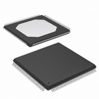
XC5210-6TQ144C Xilinx Inc, XC5210-6TQ144C Datasheet - Page 38

XC5210-6TQ144C
Manufacturer Part Number
XC5210-6TQ144C
Description
IC FPGA 324 CLB'S 144-TQFP
Manufacturer
Xilinx Inc
Series
XC5200r
Datasheet
1.XC5206-5PQ208C.pdf
(73 pages)
Specifications of XC5210-6TQ144C
Number Of Logic Elements/cells
1296
Number Of Labs/clbs
324
Number Of I /o
117
Number Of Gates
16000
Voltage - Supply
4.75 V ~ 5.25 V
Mounting Type
Surface Mount
Operating Temperature
0°C ~ 85°C
Package / Case
144-LQFP
Lead Free Status / RoHS Status
Contains lead / RoHS non-compliant
Total Ram Bits
-
Other names
122-1152
Available stocks
Company
Part Number
Manufacturer
Quantity
Price
Company:
Part Number:
XC5210-6TQ144C
Manufacturer:
XILINX
Quantity:
850
Part Number:
XC5210-6TQ144C
Manufacturer:
XILINX/赛灵思
Quantity:
20 000
XC5200 Series Field Programmable Gate Arrays
Asynchronous Peripheral Mode
Write to FPGA
Asynchronous Peripheral mode uses the trailing edge of
the logic AND condition of WS and CS0 being Low and RS
and CS1 being High to accept byte-wide data from a micro-
processor bus. In the lead FPGA, this data is loaded into a
double-buffered UART-like parallel-to-serial converter and
is serially shifted into the internal logic.
The lead FPGA presents the preamble data (and all data
that overflows the lead device) on its DOUT pin.
RDY/BUSY output from the lead FPGA acts as a hand-
shake signal to the microprocessor. RDY/BUSY goes Low
when a byte has been received, and goes High again when
the byte-wide input buffer has transferred its information
into the shift register, and the buffer is ready to receive new
data. A new write may be started immediately, as soon as
the RDY/BUSY output has gone Low, acknowledging
receipt of the previous data. Write may not be terminated
until RDY/BUSY is High again for one CCLK period. Note
that RDY/BUSY is pulled High with a high-impedance
pull-up prior to INIT going High.
The length of the BUSY signal depends on the activity in
the UART. If the shift register was empty when the new
byte was received, the BUSY signal lasts for only two
CCLK periods. If the shift register was still full when the
new byte was received, the BUSY signal can be as long as
nine CCLK periods.
Note that after the last byte has been entered, only seven
of its bits are shifted out. CCLK remains High with DOUT
equal to bit 6 (the next-to-last bit) of the last byte entered.
7-120
Figure 35:
Asynchronous Peripheral Mode Circuit Diagram
CONTROL
SIGNALS
4.7 k
Product Obsolete or Under Obsolescence
REPROGRAM
V
CC
3.3 k
4.7 k
ADDRESS
DATA
BUS
BUS
ADDRESS
DECODE
LOGIC
8
The
CS0
DONE
D0–7
CS1
RS
WS
RDY/BUSY
INIT
PROGRAM
N/C
M0
PERIPHERAL
ASYNCHRO-
3.3 k
XC5200
NOUS
M1
The READY/BUSY handshake can be ignored if the delay
from any one Write to the end of the next Write is guaran-
teed to be longer than 10 CCLK periods.
Status Read
The logic AND condition of the CS0, CS1 and RS inputs
puts the device status on the Data bus.
• D7 High indicates Ready
• D7 Low indicates Busy
• D0 through D6 go unconditionally High
It is mandatory that the whole start-up sequence be started
and completed by one byte-wide input. Otherwise, the pins
used as Write Strobe or Chip Enable might become active
outputs and interfere with the final byte transfer. If this
transfer does not occur, the start-up sequence is not com-
pleted all the way to the finish (point F in
109).
In this case, at worst, the internal reset is not released. At
best, Readback and Boundary Scan are inhibited. The
length-count value, as generated by the software, ensures
that these problems never occur.
Although RDY/BUSY is brought out as a separate signal,
microprocessors can more easily read this information on
one of the data lines. For this purpose, D7 represents the
RDY/BUSY status when RS is Low, WS is High, and the
two chip select lines are both active.
Asynchronous Peripheral mode is selected by a <101> on
the mode pins (M2, M1, M0).
DOUT
N/C
M2
CCLK
OPTIONAL
DAISY-CHAINED
FPGAs
DONE
CCLK
DIN
INIT
PROGRAM
M0
XC4000E/EX
November 5, 1998 (Version 5.2)
XC5200/
SLAVE
N/C
M1
X9006
DOUT
M2
Figure 25 on page
R


