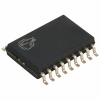
CY7C63723C-SXC Cypress Semiconductor Corp, CY7C63723C-SXC Datasheet - Page 23

CY7C63723C-SXC
Manufacturer Part Number
CY7C63723C-SXC
Description
IC MCU 8K LS USB/PS-2 18-SOIC
Manufacturer
Cypress Semiconductor Corp
Series
enCoRe™r
Datasheet
1.CY7C63723C-SXC.pdf
(53 pages)
Specifications of CY7C63723C-SXC
Package / Case
18-SOIC (7.5mm Width)
Applications
USB Microcontroller
Core Processor
M8B
Program Memory Type
OTP (8 kB)
Controller Series
CY7C637xx
Ram Size
256 x 8
Interface
PS2, USB
Number Of I /o
10
Voltage - Supply
3.5 V ~ 5.5 V
Operating Temperature
0°C ~ 70°C
Mounting Type
Surface Mount
Product
USB and PS/2 Controller
Number Of I/os
10
Operating Supply Voltage
11 V
Supply Current (max)
20 mA
Maximum Operating Temperature
+ 70 C
Minimum Operating Temperature
0 C
Mounting Style
SMD/SMT
Maximum Power Dissipation
300 mW
Number Of Timers
4
Core Size
8 Bit
No. Of I/o's
10
Program Memory Size
8KB
Ram Memory Size
256Byte
Cpu Speed
12MHz
No. Of Timers
1
Embedded Interface Type
PS/2, USB
Digital Ic Case Style
SOIC
Rohs Compliant
Yes
Lead Free Status / RoHS Status
Lead free / RoHS Compliant
Lead Free Status / RoHS Status
Lead free / RoHS Compliant, Lead free / RoHS Compliant
Other names
428-1855
Available stocks
Company
Part Number
Manufacturer
Quantity
Price
Company:
Part Number:
CY7C63723C-SXC
Manufacturer:
CYPRESS
Quantity:
12 000
Part Number:
CY7C63723C-SXC
Manufacturer:
CYPRESS/赛普拉斯
Quantity:
20 000
Master SCK Selection
The Master’s SCK is programmable to one of four clock settings,
as shown in Figure 20. The frequency is selected with the Clock
Select Bits of the SPI control register. The hardware provides 8
output clocks on the SCK pin (P0.7) for each byte transfer. Clock
phase and polarity are selected by the CPHA and CPOL control
bits (see
The master SCK duty cycle is nominally 33% in the fastest (2
Mbps) mode, and 50% in all other modes.
Operation as an SPI Slave
In slave mode, the chip receives SCK from an external master
on pin P0.7. Data from the master is shifted in on the MOSI pin
(P0.5), while data is being shifted out of the slave on the MISO
pin (P0.6). In addition, the active LOW Slave Select must be
asserted to enable the slave for transmit. The Slave Select pin is
P0.4. These pins must be configured in appropriate GPIO
modes, with the GPIO data register set to 1 to enable bypass
mode selected for the MISO pin.
In Slave mode, writes to the SPI Data Register load the Transmit
buffer. If the Slave Select is asserted (SS LOW) and the shift
register is not busy shifting a previous byte, the transmit buffer
contents will be automatically transferred into the shift register. If
the shift register is busy, the new byte will be loaded into the shift
register only after the active byte has finished and is transferred
to the receive buffer. The new byte is then ready to be shifted out
(shifting waits for SCK from the Master). If the Slave Select is not
active when the transmit buffer is loaded, data is not transferred
to the shift register until Slave Select is asserted. The Transmit
Buffer Full (TBF) bit will be set to ‘1’ until the transmit buffer’s
data-byte is transferred to the shift register. Writing to the
transmit buffer while the TBF bit is HIGH will overwrite the old
byte in the Transmit Buffer.
If the Slave Select is deasserted before a byte transfer is
complete, the transfer is aborted and no interrupt is generated.
Whenever Slave Select is asserted, the transmit buffer is
automatically reloaded into the shift register.
Clock phase and polarity must be selected to match the SPI
master, using the CPHA and CPOL control bits (see
and
The SPI slave logic continues to operate in suspend, so if the SPI
interrupt is enabled, the device can go into suspend during a SPI
slave transaction, and it will wake up at the interrupt that signals
the end of the byte transfer.
Document #: 38-08022 Rev. *D
Figure
Figure 20
23).
and 23).
Figure 22
SPI Status and Control
The SPI Control Register is shown in
diagram in
various SPI modes.
Figure 22. SPI Control Register (Address 0x61)
Bit 7: TCMP
Bit 6: TBF
Bit [5:4] Comm Mode[1:0]
Bit 3: CPOL
Bit 2: CPHA
Bit [1:0]: SCK Select
Read/Write R/W R/W R/W R/W R/W
Bit Name TCMP TBF
1 = TCMP is set to 1 by the hardware when 8-bit transfer is
complete. The SPI interrupt is asserted at the same time
TCMP is set to 1.
0 = This bit is only cleared by firmware.
Transmit Buffer Full bit.
1 = Indicates data in the transmit buffer has not transferred to
the shift register.
0 = Indicates data in the transmit buffer has transferred to the
shift register.
00 = All communications functions disabled (default).
01 = SPI Master Mode.
10 = SPI Slave Mode.
11 = Reserved.
SPI Clock Polarity bit.
1 = SCK idles HIGH.
0 = SCK idles LOW.
SPI Clock Phase bit (see
Master mode SCK frequency selection (no effect in Slave
Mode):
00 = 2 Mbit/s
01 = 1 Mbit/s
10 = 0.5 Mbit/s
11 = 0.0625 Mbit/s
Reset
Bit #
Figure 23
7
0
shows the clock and data states for the
6
0
Mode[1:0]
5
Comm
0
Figure
4
0
23)
Figure
CPOL CPHA
3
0
CY7C63722C
CY7C63723C
CY7C63743C
22. The timing
R/W R/W R/W
2
0
Page 23 of 53
1
Select
0
SCK
0
0
[+] Feedback


