CY7C66113C-PVXC Cypress Semiconductor Corp, CY7C66113C-PVXC Datasheet
CY7C66113C-PVXC
Specifications of CY7C66113C-PVXC
Available stocks


Related parts for CY7C66113C-PVXC


CY7C66113C-PVXC Summary of contents
Page 1
... The CY7C66113C has 31 GPIO pins (P0[7:0], P1[7:0], P2[7:0], P3[6:0]). DAC The CY7C66113C has an additional port P4[7:0] that features an additional eight programmable sink current I/O pins (DAC). Every DAC pin includes an integrated 14 kΩ pull up resistor. When a ‘1’ is written to a DAC I/O pin, the output current sink is disabled and the output pin is driven HIGH by the internal pull up resistor. When a ‘ ...
Page 2
... MHz clock signals for distribution within the microcontroller. Memory The CY7C66013C and CY7C66113C have PROM. Power on Reset, Watchdog, and Free Running Timer These parts include POR logic, a WDT, and a 12-bit free-running timer. The POR logic detects when power is applied to the device, resets the logic to a known state, and begins executing instructions at PROM address 0x0000 ...
Page 3
... P2[6]; CS P3[0] GPIO High Current Outputs PORT 3 P3[4] GPIO Additional P3[5] High Current PORT 3 P3[6] Outputs DAC[0] DAC PORT DAC[7] CY7C66113C only SCLK SDATA Interface 2 *I C-compatible interface enabled by firmware through P2[1:0] or P1[1:0] D+[0] Upstream USB Port D–[0] USB D+[1] D–[1] ...
Page 4
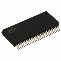
... Pin Configurations Figure 1. CY7C66013C 48-Pin SSOP and CY7C66113C 56-Pin SSOP CY7C66013C XTALOUT XTALIN V REF P1[3] P1[5] P1[7] P3[1] D+[0] D–[0] P3[3] GND D+[1] D–[1] P2[1] D+[2] D–[2] P2[3] P2[5] P2[7] GND P0[7] P0[5] P0[3] P0[1] Document Number: 38-08024 Rev. *D TOP VIEW ...
Page 5
... D+[1] 5 D–[1] 6 P2[1] 7 D+[2] 8 D–[2] 9 P2[3] 10 P2[5] 11 P2[7] 12 DAC[7] 13 P0[7] 14 Document Number: 38-08024 Rev. *D CY7C66013C, CY7C66113C Figure 2. CY7C66113C 56-Pin QFN CY7C66113C 56-Pin QFN P3[0] 42 D–[3] 41 D+[3] 40 P3[2] 39 P3[4] 38 D–[4] 37 D+[4] 36 P3[6] 35 P2[0] 34 P2[2] ...
Page 6
... Cypress Logo Pin 15 Pin 30 (0,0) Document Number: 38-08024 Rev. *D CY7C66013C, CY7C66113C Figure 3. CY7C66113C DIE Pin 1 Pin 60 Pin 45 DIE STEP: 3398 x 4194 microns Die Size: 3322 x 4129 microns Die Thickness: 14 mils = 355.6 microns Pad Size microns (3398, 4194) Page [+] Feedback ...
Page 7
... Vss 0 30 Port07 375.2 31 Port05 478.2 32 Port03 581.2 33 Port01 684.2 34 DAC5 788.4 35 DAC3 891.4 36 DAC1 994.4 Document Number: 38-08024 Rev. *D CY7C66013C, CY7C66113C Y Pad # Pin Name 3588.8 37 DAC6 3588.8 38 DAC4 3588.8 39 DAC2 3588.8 40 Port06 3588.8 41 Port04 3588.8 42 Port02 3588.8 43 Port00 3408.35 ...
Page 8
... R/W GPIO Port 2 Data R/W GPIO Port 3 Data W Interrupt Enable for Pins in Port 0 W Interrupt Enable for Pins in Port 1 W Interrupt Enable for Pins in Port 2 W Interrupt Enable for Pins in Port 3 R/W GPIO Port Configurations CY7C66013C, CY7C66113C Description Function Page Page ...
Page 9
... Hub Ports SE0 Status 0x4F Hub Ports Data 0x50 Hub Downstream Force Low 0x51 Processor Status & Control 0xFF Document Number: 38-08024 Rev. *D CY7C66013C, CY7C66113C Read/Write Function 2 R/W HAPI Width and I C Position Configuration R/W USB Device Address A R/W USB Address A, Endpoint 0 Counter ...
Page 10
... MOV X,A 41 MOV PSP,A 60 CALL addr 50-5F JMP addr 80-8F CALL addr 90-9F JZ addr A0-AF JNZ addr B0-BF Document Number: 38-08024 Rev. *D CY7C66013C, CY7C66113C Cycles Mnemonic 7 NOP 4 INC A 6 INC X 7 INC [expr] 4 INC [X+expr] 6 DEC A 7 DEC X 4 DEC [expr] 6 ...
Page 11
... RET instruction. The program counter is not accessed directly by the firmware. The program stack is examined by reading SRAM from location 0x00 and up. Document Number: 38-08024 Rev. *D CY7C66013C, CY7C66113C Program Memory Organization Figure 4. Program Memory Space with Interrupt Vector Table After Address ...
Page 12
... Example assembly instructions to do this with two device addresses (FIFOs begin at 0xD8) are shown: ■ MOV A,20h; Move 20 hex into Accumulator (must be D8h or less) ■ SWAP A,DSP; swap accumulator value into DSP register. Table 14. CY7C66013C, CY7C66113C [2] USB Device Endpoints on page 38. Page [+] Feedback ...
Page 13
... Address Modes The CY7C66013C and CY7C66113C microcontrollers support three addressing modes for instructions that require data operands: data, direct, and indexed. Data (Immediate) “Data” address mode refers to a data operand that is actually a constant encoded in the instruction example, consider the instruction that loads A with the constant 0xD8: MOV A, 0D8h ...
Page 14
... WDR bit, the WDR bit should be ignored if the POR (bit 3 of register 0xFF) bit is set. Figure 6. Watchdog Reset WATCH No write to WDT Execution begins at register, so WDR Reset Vector 0x0000 goes HIGH CY7C66013C, CY7C66113C drops below CC rises above minimum) of the last clear. Bit WATCH USB Device Page ...
Page 15
... This executes before any ISR Figure 7. Block Diagram of a GPIO Pin V CC mode 2-bits Q2 Q1 Data Out Latch 14 kΩ Q3* Data In Latch Data Interrupt Latch Figure 8 through Figure CY7C66013C, CY7C66113C GPIO PIN *Port 0,1,2: Low I sink Port 3: High I sink 11, and are set reset. Page [+] Feedback ...
Page 16
... Therefore unused port bit is programmed in open-drain mode, it must be written with a ‘0.’ Notice that the CY7C66013C always requires that P3[7:5] be written with a ‘0.’ When the CY7C66113C is used the P3[7] should be written with a ‘0.’ Document Number: 38-08024 Rev. *D Figure 8 ...
Page 17
... Q1, Q2, and Q3 are all OFF. The GPIO pin is not driven internally. In this mode, the pin may serve as an input. Reading the Port Data Register returns the actual logic value on the port pins. CY7C66013C, CY7C66113C (Figure 12) and the Interrupt Enable bit ADDRESS 0x08 ...
Page 18
... Enable Enable Figure 16. Port 3 Interrupt Enable P3.5 Intr P3.4 Intr P3.3 Intr Enable Enable Enable CY7C66113C only CY7C66013C, CY7C66113C GPIO and ADDRESS 0x04 P0.2 Intr P0.1 Intr P0.0 Intr Enable Enable Enable ADDRESS 0x05 P1.2 Intr P1.1 Intr P1.0 Intr Enable ...
Page 19
... DAC Port The CY7C66113CC features a programmable sink current 8-bit port, which is also known as DAC port. Each of these port I/O pins have a programmable current sink. Writing a ‘1’ DAC I/O pin disables the output current sink (I HIGH through an integrated 14 kΩ resistor. When a ‘0’ is written to a DAC I/O pin, the I disabled ...
Page 20
... All of the DAC Port Interrupt Polarity register bits are cleared during a reset. Figure 21. DAC Port Interrupt Polarity CY7C66013C, CY7C66113C ADDRESS 0x38 –0x3F Isink[2] Isink[1] Isink[ ...
Page 21
... Timer Bit 4 Timer Bit Figure 23. Timer MSB Register Reserved Reserved Timer Bit Figure 24. Timer Block Diagram CY7C66013C, CY7C66113C ADDRESS 0x24 Timer Bit 2 Timer Bit 1 Timer Bit ADDRESS 0x25 Timer Bit 10 Timer Bit 9 Timer Bit 1.024 ms interrupt μ 128 s interrupt 1 MHz clock ...
Page 22
... Drain mode, regardless of the settings of the GPIO Configuration (HAPI). Register. The electrical characteristics of the I interface is the same as that of GPIO ports 1 and 2. Note that the (max All control of the Status and compatible block. CY7C66013C, CY7C66113C 2 C compatible, and a HAPI for [3] Figure 25) . All bits of ADDRESS 0x09 Data HAPI Port ...
Page 23
... R/W R/W R Table 9, with a more detailed description following. Description 2 C compatible function is enabled. When cleared Stop bit detected (unless firmware did not ACK the 2 C compatible block is busy with a transaction, 0 when transaction is complete. CY7C66013C, CY7C66113C ADDRESS 0x29 Data Data Data 0 R/W ...
Page 24
... I these pins are free to function as GPIOs mode, the two pins operate in open drain mode, independent of 2 the GPIO configuration setting. C address CY7C66013C, CY7C66113C 2 C compatible bus at the ACK bit time compatible block during the first byte start or restart. The Addr ...
Page 25
... The Data Ready bit reads the opposite state from the external DReadyPin on pin P2[3]. If the DRDY Polarity bit is 0, DReadyPin is active HIGH, and the Data Ready bit is active LOW. Document Number: 38-08024 Rev. *D CY7C66013C, CY7C66113C Table 10 describes these signals and the HAPI control bits in the HAPI Description (Port 2 Pin) Ready for more input data from external interface ...
Page 26
... During a WDR, the Processor Status and Control Register is set to 01XX0001, which indicates a WDR (bit 6 set) has occurred and no interrupts are pending (bit 7 clear). The WDR does not effect the state of the POR and the Bus Reset Interrupt bits. CY7C66013C, CY7C66113C ADDRESS 0xFF 2 1 ...
Page 27
... When an interrupt is generated first registered as a pending interrupt. It stays pending until it is serviced or a reset occurs. A pending interrupt only generates an interrupt request enabled by the corresponding bit in the interrupt enable registers. The highest priority interrupt request CY7C66013C, CY7C66113C ADDRESS 0X20 128 μ ...
Page 28
... AddrB EP1 IRQ Hub CLR Hub IRQ DAC CLR DAC IRQ GPIO/HAPI CLR GPIO/HAPI IRQ CLR IRQ Interrupt Priority Encoder CY7C66013C, CY7C66113C To CPU CPU IRQ Sense IRQ Global Int Enable Interrupt Sense Enable Bit Controlled by DI, EI, and CLR RETI Instructions Interrupt ...
Page 29
... USB repeater hardware. The babble and resume events are additionally gated by the corresponding bits of the Hub Port Enable Register disconnect event on a port does not generate an interrupt if the SIE does not drive the port (that is, the port is being forced). CY7C66013C, CY7C66113C Function Power on Reset on page 14. (Figure 35) ...
Page 30
... GPIO bits, including ports and bits not used by HAPI. Operation of the HAPI interrupt Document Number: 38-08024 Rev. *D CY7C66013C, CY7C66113C GPIO and HAPI Interrupt Each of the GPIO pins generates an interrupt, if enabled. The interrupt polarity is programmed for each GPIO port as part of the GPIO configuration ...
Page 31
... Firmware responds by sending the Device descriptor over the USB bus, via the on-chip FIFOs. 4. After receiving the descriptor, the host sends a SETUP packet followed by a DATA packet to address 0 assigning a new USB address to the device. CY7C66013C, CY7C66113C must be ext the CY7C66x13C microcontroller ...
Page 32
... The Hub Ports Connect Status register is cleared to zero by reset or USB bus reset, then set to match the hardware configuration by the hub repeater hardware. The Reserved bits [7..4] should always read as ‘0’ to indicate no connection. CY7C66013C, CY7C66113C connected between its UUP to indicate full speed USB ...
Page 33
... Babble is defined as: ■ Any non idle downstream traffic on an enabled downstream port at EOF2 ■ Any downstream port with upstream connectivity established at EOF2 (that is, no EOP received by EOF2). CY7C66013C, CY7C66113C ADDRESS 0x4A R/W R/W R ADDRESS 0x49 ...
Page 34
... Control Action Figure 37. Hub Ports Force Low Register Force Low Force Low Force Low D+[3] D–[3] D+[2] R/W R/W R CY7C66013C, CY7C66113C may cause current flow into REF ADDRESS 0x4B Port 2 Port 1 Port 1 Control Bit 0 Control Bit 1 Control Bit 0 R/W R/W R/W 0 ...
Page 35
... Bit 7: Device Remote Wakeup. When set to 1, Enable hardware upstream resume signaling for connect and disconnect events during global resume. When set to 0, Disable hardware upstream resume signaling for connect and disconnect events during global resume. CY7C66013C, CY7C66113C ADDRESS 0x4F Port 3 ...
Page 36
... All allowed port changes wake the part. Then, the part uses internal timing to determine whether to take action or return to suspend. If Device Remote Wakeup is set, automatic hardware assertions take place on Resume events. CY7C66013C, CY7C66113C ADDRESS 0x4E ...
Page 37
... USB Device Endpoints Bit 7: Endpoint Size This bit used to configure the number of USB endpoints. See USB Device Endpoints The hub generates an EOP at EOF1 in accordance with the USB 1.1 Specification, Section 11.2.2. CY7C66013C, CY7C66113C Figure 42. All bits in the register are cleared ADDRESS 0x1F 2 ...
Page 38
... IN or OUT endpoints. The endpoint mode registers are cleared during reset. When USB Status And Control Register Bits [6,7] are set to [0,0] or [1,0], the endpoint 0 EPA0 and EPB0 mode registers use the format shown in CY7C66013C, CY7C66113C ADDRESSES 0x10(A) and 0x40( ...
Page 39
... Nak in” mode. Therefore, if following the status stage of a Control Write transfer a USB host were to immediately start the next transfer, the new Setup packet could override the data payload of the data stage of the previous Control Write. CY7C66013C, CY7C66113C ADDRESSES 0x12(A0) and 0x42(B0) 2 ...
Page 40
... SETUP or OUT transactions before firmware has a chance to read the data. Only endpoint 0 counter register is locked when updated. The locking mechanism does not apply to the count registers of other endpoints. CY7C66013C, CY7C66113C ADDRESSES 0x14, 0x16, 0x44 Mode Bit 2 ...
Page 41
... UPDATE. The firmware needs to perform a register read as a part of the endpoint ISR processing to unlock Document Number: 38-08024 Rev. *D CY7C66013C, CY7C66113C the effected registers. The locking mechanism on mode and counter registers ensures that the firmware recognizes the changes that the SIE might have made since the previous I/O read of that register ...
Page 42
... C Data Packet UPDATE Host To Device Data 1/0 Data Packet UPDATE SETUP Host To Device Data 1/0 Data Packet UPDATE only if FIFO is CY7C66013C, CY7C66113C Host To Device Hand Shake Packet UPDATE Device To Host E S ACK, Y NAK, N STAL C Hand Shake Packet written Page [+] Feedback ...
Page 43
... Bits [3:0] are set to '1111' which is ACK IN-Status OUT mode as shown in Table 14, the SIE changes the endpoint Mode Bits [3:0] to NAK IN-Status OUT mode (1110) after ACK’ing a valid status USB Non Control Endpoint Mode Registers CY7C66013C, CY7C66113C Comments on page 40. Page [+] Feedback ...
Page 44
... USB request). This read unlocks the register. So care must be taken not to overwrite the register elsewhere. CY7C66013C, CY7C66113C Interrupt In Out ACK ...
Page 45
... Changes made by SIE to Internal Registers and Mode Bits dval DTOG DVAL COUNT Setup 1 1 updates updates UC updates 1 updates CY7C66013C, CY7C66113C In Out ACK Mode Bits Response ACK Change ignore Change ignore In Out ACK Mode Bits Response Change ignore Change NAK Change NAK ...
Page 46
... ENDPOINT Changes made by SIE to Internal Registers and Mode Bits dval DTOG DVAL COUNT Setup CY7C66013C, CY7C66113C Change ACK Stall Stall Change ignore Change ignore Change NAK Change ACK Stall Stall Change ignore Change ignore Stall In Out ACK Mode Bits Response ACK ...
Page 47
... Count Count Count Bit 5 Bit 4 Bit 3 Bit 2 - ACK Mode Bit 3 Mode Bit 2 Mode Bit 1 Mode Bit 0 bbbbbbbb D+ D– Bus Control Upstream Upstream Activity Bit 2 CY7C66013C, CY7C66113C Change NAK yes UC No Change ignore Change TX yes Read/Write/ Default/ Bit 1 Bit 0 [ Both Reset P0 ...
Page 48
... Force Low Force Low Force Low Force Low D+[3] D–[3] D+[2] D–[2] USB Bus Power-on Suspend Interrupt Reset In- Reset Enable terrupt Sense CY7C66013C, CY7C66113C Read/Write/ Bit 2 Bit 1 Bit 0 [ Both 128 μs USB Bus -bbbbbbb -0000000 Interrupt RESET In- Enable terrupt En- able ...
Page 49
... Figure 48. Sample Schematic Vref 2.2 μF 0.01 μF 0.01 μF 22x8(R ) ext D1– D1+ D2– D2+ D3– D3+ D4– D4+ 15K(x8 UDN POWER MANAGEMENT CY7C66013C, CY7C66113C USB-A Vbus D– D+ GND USB-A Vbus D– D+ GND USB-A Vbus D– D+ GND USB-A Vbus D– D+ GND Page ...
Page 50
... USB pins [10] Linear ramp kΩ ±5% to Gnd 1.5 kΩ ± REF Including R Resistor ext All ports, LOW to HIGH edge All ports, HIGH to LOW edge below approximately 2.5V. CC CY7C66013C, CY7C66113C CC = 4.0V to 5.25V) CC Min Max Unit 3.15 3.45 V –0.4 0 μ μ ...
Page 51
... V = 2.0V DC out V = 2.0V DC out V = 2.0V DC out [11 2.0V DC out [12 2.0V out V = 2.0V DC out [13] DAC Port = 6.0 MHz) Description / [15, 16] [16] [15, 16] CY7C66013C, CY7C66113C = 4.0V to 5.25V) (continued) CC Min Max Unit 2.4 V 8.0 24.0 kΩ 0.1 0.3 mA 0.5 1.5 mA 1.6 4 1.6 4.8 mA 0.6 LSB ...
Page 52
... STB LOW to Latch_Empty Deasserted STBLE Timer Signals t WDT Period watch CLOCK D+ D− Document Number: 38-08024 Rev 6.0 MHz) Description [16] [16] [15, 16] Figure 49. Clock Timing t CYC Figure 50. USB Data Signal Timing 90% 90% 10% CY7C66013C, CY7C66113C Min Max Unit 8.192 14.336 ms 10% Page [+] Feedback ...
Page 53
... Figure 51. HAPI Read by External Interface from USB Microcontroller Interrupt Generated CS (P2.6, input) OE (P2.5, input) DATA (output) STB (P2.4, input) DReadyPin (P2.3, output) (Shown for DRDY Polarity=0) Internal Write Internal Addr Document Number: 38-08024 Rev D[23:0] t OED t OEDR (Ready) Port0 CY7C66013C, CY7C66113C Int t OEZ Page [+] Feedback ...
Page 54
... DATA (input) OE (P2.5, input) LEmptyPin (P2.2, output) (Shown for LEMPTY Polarity=0) Internal Read Internal Addr Ordering Information Ordering Code PROM Size CY7C66013C-PVXC 8 KB CY7C66113C-PVXC 8 KB CY7C66113C-LFXC 8 KB CY7C66113C-PVXCT 8 KB CY7C66113C- CY7C66113C-LTXC 8 KB CY7C66113C-LTXCT 8 KB Document Number: 38-08024 Rev. *D CY7C66013C, CY7C66113C STBZ D[23:0] ...
Page 55
... Package Diagrams Figure 53. 48-Pin Shrunk Small Outline Package O48 Figure 54. 56-Pin Shrunk Small Outline Package O56 Document Number: 38-08024 Rev. *D CY7C66013C, CY7C66113C 51-85061-*C 51-85062-*C Page [+] Feedback ...
Page 56
... Document Number: 38-08024 Rev. *D Figure 55. 56-Pin QFN LF56A CY7C66013C, CY7C66113C 51-85144 *G Page [+] Feedback ...
Page 57
... Figure 56. 56-QFN 8x8x0.9 mm EPad 6.1x6.1 mm Document Number: 38-08024 Rev. *D CY7C66013C, CY7C66113C 51-85187 *C Page [+] Feedback ...
Page 58
... QFN to the circuit board ground plane. Figure 58. Plot of the Solder Mask (White Area) Document Number: 38-08024 Rev. *D CY7C66013C, CY7C66113C For further information on this package design please refer to the application note Surface Mount Assembly of AMKOR’s MicroLeadFrame (MLF) Technology. This application note can be downloaded from AMKOR’ ...
Page 59
... Document History Page Document Title: CY7C66013C, CY7C66113C Full Speed USB (12 Mbps) Peripheral Controller with Integrated Hub Document Number: 38-08024 Submission Rev. ECN No. Date ** 114525 3/27/02 *A 124768 03/20/03 *B 417632 See ECN *C 1825466 See ECN TLY/PYRS Changed Title from "CY7C66013, CY7C66113 Full Speed USB (12 Mbps) ...