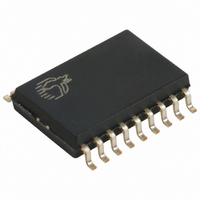
CY7C63723-SXC Cypress Semiconductor Corp, CY7C63723-SXC Datasheet - Page 14

CY7C63723-SXC
Manufacturer Part Number
CY7C63723-SXC
Description
IC MCU 8K LS USB/PS-2 18-SOIC
Manufacturer
Cypress Semiconductor Corp
Series
enCoRe™r
Specifications of CY7C63723-SXC
Applications
USB Microcontroller
Core Processor
M8B
Program Memory Type
OTP (8 kB)
Controller Series
CY7C637xx
Ram Size
256 x 8
Interface
PS2, USB
Number Of I /o
10
Voltage - Supply
4 V ~ 5.5 V
Operating Temperature
0°C ~ 70°C
Mounting Type
Surface Mount
Package / Case
18-SOIC (7.5mm Width)
Lead Free Status / RoHS Status
Lead free / RoHS Compliant
Other names
428-1720-5
CY7C63723-SXC
CY7C63723-SXC
Available stocks
Company
Part Number
Manufacturer
Quantity
Price
Company:
Part Number:
CY7C63723-SXC
Manufacturer:
NS
Quantity:
16
Part Number:
CY7C63723-SXC
Manufacturer:
CYPRESS/赛普拉斯
Quantity:
20 000
Table 11-1. Wake-up Timer Adjust Settings
12.0
Ports 0 and 1 provide up to 16 versatile GPIO pins that can be
read or written (the number of pins depends on package type).
Figure 12-1 shows a diagram of a GPIO port pin.
Port 0 is an 8-bit port; Port 1 contains either 2 bits, P1.1–P1.0
in the CY7C63723, or all 8 bits, P1.7–P1.0 in the CY7C63743
parts. Each bit can also be selected as an interrupt source for
the microcontroller, as explained in Section 21.0.
The data for each GPIO pin is accessible through the Port
Data register. Writes to the Port Data register store outgoing
data state for the port pins, while reads from the Port Data
register return the actual logic value on the port pins, not the
Port Data register contents.
Document #: 38-08022 Rev. *B
SPI Bypass (P0.5–P0.7 only)
(=1 if SPI inactive, or for non-SPI pins)
(Bits [6:4] in Figure 9-2)
Adjust Bits [2:0]
000 (reset state)
General Purpose I/O Ports
See Section 26.0 for the value of t
Internal
Data Bus
001
010
011
100
101
110
111
GPIO
Mode
Interrupt
Polarity
Interrupt
Enable
Port Write
Data
Out
Register
Figure 12-1. Block Diagram of GPIO Port (one pin shown)
Port Read
FOR
FOR
Wake-up Time
2
(Data Reg must be 1
for SPI outputs)
128 * t
16 * t
32 * t
64 * t
1 * t
2 * t
4 * t
8 * t
WAKE
WAKE
WAKE
WAKE
WAKE
WAKE
WAKE
WAKE
WAKE
Interrupt
Logic
Threshold Select
Each GPIO pin is configured independently. The driving state
of each GPIO pin is determined by the value written to the pin’s
Data Register and by two associated pin’s Mode0 and Mode1
bits.
The Port 0 Data Register is shown in Figure 12-2, and the Port
1 Data Register is shown in Figure 12-3. The Mode0 and
Mode1 bits for the two GPIO ports are given in Figure 12-4
through Figure 12-7.
To Interrupt
Controller
Q1
Q2
14 k Ω
V
CC
Q3
To Capture Timers (P0.0, P0.1)
and SPI (P0.4–P0.7))
GPIO
Pin
CY7C63722
CY7C63723
CY7C63743
Page 14 of 49


